LPC2294HBD144/01,5 NXP Semiconductors, LPC2294HBD144/01,5 Datasheet - Page 12
LPC2294HBD144/01,5
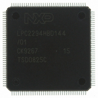
Manufacturer Part Number
LPC2294HBD144/01,5
Description
IC ARM7 MCU FLASH 256K 144-LQFP
Manufacturer
NXP Semiconductors
Series
LPC2200r
Datasheet
1.LPC2292FBD144015.pdf
(53 pages)
Specifications of LPC2294HBD144/01,5
Program Memory Type
FLASH
Program Memory Size
256KB (256K x 8)
Package / Case
144-LQFP
Core Processor
ARM7
Core Size
16/32-Bit
Speed
60MHz
Connectivity
CAN, EBI/EMI, I²C, Microwire, SPI, SSI, SSP, UART/USART
Peripherals
POR, PWM, WDT
Number Of I /o
112
Ram Size
16K x 8
Voltage - Supply (vcc/vdd)
1.65 V ~ 3.6 V
Data Converters
A/D 8x10b
Oscillator Type
Internal
Operating Temperature
-40°C ~ 125°C
Processor Series
LPC22
Core
ARM7TDMI-S
Data Bus Width
16 bit, 32 bit
Data Ram Size
16 KB
Interface Type
CAN/I2C/JTAG/SPI/SSP/UART
Maximum Clock Frequency
60 MHz
Number Of Programmable I/os
112
Number Of Timers
2
Operating Supply Voltage
3.3 V
Maximum Operating Temperature
+ 125 C
Mounting Style
SMD/SMT
3rd Party Development Tools
MDK-ARM, RL-ARM, ULINK2
Development Tools By Supplier
OM10068
Minimum Operating Temperature
- 40 C
On-chip Adc
8-ch x 10-bit
Package
144LQFP
Device Core
ARM7TDMI-S
Family Name
LPC2000
Maximum Speed
60 MHz
Lead Free Status / RoHS Status
Lead free / RoHS Compliant
For Use With
OM10091 - KIT DEV PHYCORE-ARM7/LPC2220622-1005 - USB IN-CIRCUIT PROG ARM7 LPC2K568-1757 - BOARD EVAL FOR LPC220X ARM MCU
Eeprom Size
-
Lead Free Status / Rohs Status
Lead free / RoHS Compliant
Other names
568-4321
935284877551
LPC2294HBD144/01-S
LPC2294HBD144/01-S
935284877551
LPC2294HBD144/01-S
LPC2294HBD144/01-S
Available stocks
Company
Part Number
Manufacturer
Quantity
Price
Company:

Part Number:
LPC2294HBD144/01,5
Manufacturer:
NXP Semiconductors
Quantity:
10 000


NXP Semiconductors
Table 4.
LPC2292_2294_7
Product data sheet
Symbol
P2[24]/D24
P2[25]/D25
P2[26]/D26/
BOOT0
P2[27]/D27/
BOOT1
P2[28]/D28
P2[29]/D29
P2[30]/D30/
AIN4
P2[31]/D31/
AIN5
P3[0] to P3[31]
P3[0]/A0
P3[1]/A1
P3[2]/A2
P3[3]/A3
P3[4]/A4
P3[5]/A5
P3[6]/A6
P3[7]/A7
P3[8]/A8
P3[9]/A9
P3[10]/A10
P3[11]/A11
P3[12]/A12
P3[13]/A13
P3[14]/A14
P3[15]/A15
P3[16]/A16
Pin description
Pin (LQFP)
11
12
13
16
17
18
19
20
89
88
87
81
80
74
73
72
71
66
65
64
63
62
56
55
53
[7]
[7]
[7]
[7]
[7]
[7]
[6]
[6]
[7]
[7]
[7]
[7]
[7]
[7]
[7]
[7]
[7]
[7]
[7]
[7]
[7]
[7]
[7]
[7]
[7]
…continued
Pin
(TFBGA)
E2
E1
F4
F1
G2
G1
G3
G4
G12
H13
H12
J10
K13
M13
N13
M12
N12
M10
N10
K9
L9
M9
K7
L7
M7
[7]
[7]
[7]
[7]
[7]
[7]
[7]
[7]
[7]
[7]
[6]
[6]
[7]
[7]
[7]
[7]
[7]
[7]
[7]
[7]
[7]
[7]
[7]
[7]
[7]
[1]
Type
I/O
I/O
I/O
I
I/O
I
I/O
I/O
I/O
I
I/O
I
I/O
O
O
O
O
O
O
O
O
O
O
O
O
O
O
O
O
O
Rev. 7 — 4 December 2008
16/32-bit ARM microcontrollers with external memory interface
Description
D24 — External memory data line 24.
D25 — External memory data line 25.
D26 — External memory data line 26.
BOOT0 — While RESET is low, together with BOOT1 controls
booting and internal operation. Internal pull-up ensures high
state if pin is left unconnected.
D27 — External memory data line 27.
BOOT1 — While RESET is low, together with BOOT0 controls
booting and internal operation. Internal pull-up ensures high
state if pin is left unconnected.
BOOT1:0 = 00 selects 8-bit memory on CS0 for boot.
BOOT1:0 = 01 selects 16-bit memory on CS0 for boot.
BOOT1:0 = 10 selects 32-bit memory on CS0 for boot.
BOOT1:0 = 11 selects internal flash memory.
D28 — External memory data line 28.
D29 — External memory data line 29.
D30 — External memory data line 30.
AIN4 — ADC, input 4. This analog input is always connected
to its pin.
D31 — External memory data line 31.
AIN5 — ADC, input 5. This analog input is always connected
to its pin.
Port 3 — Port 3 is a 32-bit bidirectional I/O port with individual
direction controls for each bit. The operation of port 3 pins
depends upon the pin function selected via the Pin Connect
Block.
A0 — External memory address line 0.
A1 — External memory address line 1.
A2 — External memory address line 2.
A3 — External memory address line 3.
A4 — External memory address line 4.
A5 — External memory address line 5.
A6 — External memory address line 6.
A7 — External memory address line 7.
A8 — External memory address line 8.
A9 — External memory address line 9.
A10 — External memory address line 10.
A11 — External memory address line 11.
A12 — External memory address line 12.
A13 — External memory address line 13.
A14 — External memory address line 14.
A15 — External memory address line 15.
A16 — External memory address line 16.
LPC2292/LPC2294
© NXP B.V. 2008. All rights reserved.
12 of 53
Related parts for LPC2294HBD144/01,5
Image
Part Number
Description
Manufacturer
Datasheet
Request
R

Part Number:
Description:
NXP Semiconductors designed the LPC2420/2460 microcontroller around a 16-bit/32-bitARM7TDMI-S CPU core with real-time debug interfaces that include both JTAG andembedded trace
Manufacturer:
NXP Semiconductors
Datasheet:

Part Number:
Description:
NXP Semiconductors designed the LPC2458 microcontroller around a 16-bit/32-bitARM7TDMI-S CPU core with real-time debug interfaces that include both JTAG andembedded trace
Manufacturer:
NXP Semiconductors
Datasheet:
Part Number:
Description:
NXP Semiconductors designed the LPC2468 microcontroller around a 16-bit/32-bitARM7TDMI-S CPU core with real-time debug interfaces that include both JTAG andembedded trace
Manufacturer:
NXP Semiconductors
Datasheet:
Part Number:
Description:
NXP Semiconductors designed the LPC2470 microcontroller, powered by theARM7TDMI-S core, to be a highly integrated microcontroller for a wide range ofapplications that require advanced communications and high quality graphic displays
Manufacturer:
NXP Semiconductors
Datasheet:
Part Number:
Description:
NXP Semiconductors designed the LPC2478 microcontroller, powered by theARM7TDMI-S core, to be a highly integrated microcontroller for a wide range ofapplications that require advanced communications and high quality graphic displays
Manufacturer:
NXP Semiconductors
Datasheet:
Part Number:
Description:
The Philips Semiconductors XA (eXtended Architecture) family of 16-bit single-chip microcontrollers is powerful enough to easily handle the requirements of high performance embedded applications, yet inexpensive enough to compete in the market for hi
Manufacturer:
NXP Semiconductors
Datasheet:
Part Number:
Description:
The XA-S3 device is a member of Philips Semiconductors? XA(eXtended Architecture) family of high performance 16-bitsingle-chip microcontrollers
Manufacturer:
NXP Semiconductors
Datasheet:

Part Number:
Description:
The NXP BlueStreak LH75401/LH75411 family consists of two low-cost 16/32-bit System-on-Chip (SoC) devices
Manufacturer:
NXP Semiconductors
Datasheet:
Part Number:
Description:
The NXP LPC3130/3131 combine an 180 MHz ARM926EJ-S CPU core, high-speed USB2
Manufacturer:
NXP Semiconductors
Datasheet:
Part Number:
Description:
The NXP LPC3141 combine a 270 MHz ARM926EJ-S CPU core, High-speed USB 2
Manufacturer:
NXP Semiconductors
Part Number:
Description:
The NXP LPC3143 combine a 270 MHz ARM926EJ-S CPU core, High-speed USB 2
Manufacturer:
NXP Semiconductors

Part Number:
Description:
The NXP LPC3152 combines an 180 MHz ARM926EJ-S CPU core, High-speed USB 2
Manufacturer:
NXP Semiconductors
Part Number:
Description:
The NXP LPC3154 combines an 180 MHz ARM926EJ-S CPU core, High-speed USB 2
Manufacturer:
NXP Semiconductors

Part Number:
Description:
Standard level N-channel enhancement mode Field-Effect Transistor (FET) in a plastic package using NXP High-Performance Automotive (HPA) TrenchMOS technology
Manufacturer:
NXP Semiconductors
Datasheet: