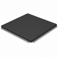
LPC2478FBD208,551 NXP Semiconductors, LPC2478FBD208,551 Datasheet - Page 10

LPC2478FBD208,551
Manufacturer Part Number
LPC2478FBD208,551
Description
IC ARM7 MCU 512K LCD 208-LQFP
Manufacturer
NXP Semiconductors
Series
LPC2400r
Datasheets
1.OM11077.pdf
(91 pages)
2.OM11077.pdf
(792 pages)
3.OM11077.pdf
(10 pages)
4.LPC2478FBD208551.pdf
(89 pages)
Specifications of LPC2478FBD208,551
Program Memory Type
FLASH
Program Memory Size
512KB (512K x 8)
Package / Case
208-LQFP
Core Processor
ARM7
Core Size
16/32-Bit
Speed
72MHz
Connectivity
CAN, EBI/EMI, Ethernet, I²C, Microwire, MMC, SPI, SSI, SSP, UART/USART, USB OTG
Peripherals
Brown-out Detect/Reset, DMA, I²S, LCD, POR, PWM, WDT
Number Of I /o
160
Ram Size
96K x 8
Voltage - Supply (vcc/vdd)
3 V ~ 3.6 V
Data Converters
A/D 8x10b; D/A 1x10b
Oscillator Type
Internal
Operating Temperature
-40°C ~ 85°C
Processor Series
LPC24
Core
ARM7TDMI-S
Data Bus Width
16 bit, 32 bit
Data Ram Size
98 KB
Interface Type
CAN/I2C/I2S/IrDA/SPI/SSP/UART/USB
Maximum Clock Frequency
72 MHz
Number Of Programmable I/os
160
Number Of Timers
4
Operating Supply Voltage
3.3 V
Maximum Operating Temperature
+ 85 C
Mounting Style
SMD/SMT
3rd Party Development Tools
MDK-ARM, RL-ARM, ULINK2, DK-35TS-LPC2478, DK-57TS-LPC2478, DK-57VTS-LPC2478, SOMDIMM-LPC2478, SAB-TFBGA208, KSK-LPC2478-JL, MCB2470
Development Tools By Supplier
OM11015, OM11019, OM11022
Minimum Operating Temperature
- 40 C
On-chip Adc
8-ch x 10-bit
On-chip Dac
1-ch x 10-bit
Lead Free Status / RoHS Status
Lead free / RoHS Compliant
For Use With
622-1034 - PROGRAMMERS, DEVELOPMENT SYSTEMS622-1033 - KIT LCD TOUCH 5.7" FOR LPC2478MCB2470 - BOARD EVAL NXP LPC247X SERIESOM11022 - EVAL LPC-STICK WITH LPC2478OM11019 - BOARD EVAL FOR LPC2478568-4742 - MODULE DIMM LPC2478 ARM7568-4741 - KIT LCD TOUCH 5.7" FOR LPC2478622-1028 - KIT LCD TOUCH 5.7" FOR LPC2478KSDKLPC2478-PL - KIT IAR KICKSTART NXP LPC2478622-1024 - BOARD SCKT ADAPTER FOR TFBGA208568-4369 - BOARD EVAL FOR LPC2478622-1005 - USB IN-CIRCUIT PROG ARM7 LPC2K
Eeprom Size
-
Lead Free Status / Rohs Status
Lead free / RoHS Compliant
Other names
568-4363
935284069551
LPC2478FBD208-S
935284069551
LPC2478FBD208-S
Available stocks
Company
Part Number
Manufacturer
Quantity
Price
Company:
Part Number:
LPC2478FBD208,551
Manufacturer:
NXP Semiconductors
Quantity:
10 000
Part Number:
LPC2478FBD208,551
Manufacturer:
NXP/恩智浦
Quantity:
20 000
NXP Semiconductors
Table 4.
LPC2478
Product data sheet
Symbol
P0[0] to P0[31]
P0[0]/RD1/TXD3/
SDA1
P0[1]/TD1/RXD3/
SCL1
P0[2]/TXD0
P0[3]/RXD0
P0[4]/I2SRX_CLK/
LCDVD[0]/RD2/
CAP2[0]
P0[5]/I2SRX_WS/
LCDVD[1]/TD2/
CAP2[1]
P0[6]/I2SRX_SDA/
LCDVD[8]/
SSEL1/MAT2[0]
Pin description
6.2 Pin description
Pin
94
96
202
204
168
166
164
[1]
[1]
[1]
[1]
[1]
[1]
[1]
Ball
U15
T14
C4
D6
B12
C12
D13
[1]
[1]
[1]
[1]
[1]
[1]
[1]
All information provided in this document is subject to legal disclaimers.
Type
I/O
I/O
I
O
I/O
I/O
O
I
I/O
I/O
O
I/O
I
I/O
I/O
O
I
I
I/O
I/O
O
O
I
I/O
I/O
O
I/O
O
Rev. 2 — 29 September 2010
Description
Port 0: Port 0 is a 32-bit I/O port with individual direction controls for each
bit. The operation of port 0 pins depends upon the pin function selected
via the pin connect block.
P0[0] — General purpose digital input/output pin.
RD1 — CAN1 receiver input.
TXD3 — Transmitter output for UART3.
SDA1 — I
P0[1] — General purpose digital input/output pin.
TD1 — CAN1 transmitter output.
RXD3 — Receiver input for UART3.
SCL1 — I
P0[2] — General purpose digital input/output pin.
TXD0 — Transmitter output for UART0.
P0[3] — General purpose digital input/output pin.
RXD0 — Receiver input for UART0.
P0[4] — General purpose digital input/output pin.
I2SRX_CLK — I
by the slave. Corresponds to the signal SCK in the I2S-bus
specification.
LCDVD[0] — LCD data.
RD2 — CAN2 receiver input.
CAP2[0] — Capture input for Timer 2, channel 0.
P0[5] — General purpose digital input/output pin.
I2SRX_WS — I
received by the slave. Corresponds to the signal WS in the I
specification.
LCDVD[1] — LCD data.
TD2 — CAN2 transmitter output.
CAP2[1] — Capture input for Timer 2, channel 1.
P0[6] — General purpose digital input/output pin.
I2SRX_SDA — I
by the receiver. Corresponds to the signal SD in the I
specification.
LCDVD[8] — LCD data.
SSEL1 — Slave Select for SSP1.
MAT2[0] — Match output for Timer 2, channel 0.
2
2
C1 clock input/output (this is not an open-drain pin).
C1 data input/output (this is not an open-drain pin).
[17]
[17]
[17]
2
2
S Receive word select. It is driven by the master and
2
S Receive clock. It is driven by the master and received
S Receive data. It is driven by the transmitter and read
[17]
[17]
[17]
Single-chip 16-bit/32-bit microcontroller
LPC2478
2
© NXP B.V. 2010. All rights reserved.
S-bus
2
S-bus
10 of 91


