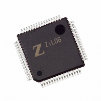
Z16F2810AG20SG Zilog, Z16F2810AG20SG Datasheet - Page 28

Z16F2810AG20SG
Manufacturer Part Number
Z16F2810AG20SG
Description
IC ZNEO MCU FLASH 128K 64LQFP
Manufacturer
Zilog
Series
Encore!® ZNEOr
Specifications of Z16F2810AG20SG
Core Processor
ZNEO
Core Size
16-Bit
Speed
20MHz
Connectivity
I²C, IrDA, LIN, SPI, UART/USART
Peripherals
Brown-out Detect/Reset, DMA, POR, PWM, WDT
Number Of I /o
46
Program Memory Size
128KB (128K x 8)
Program Memory Type
FLASH
Ram Size
4K x 8
Voltage - Supply (vcc/vdd)
2.7 V ~ 3.6 V
Data Converters
A/D 12x10b
Oscillator Type
Internal
Operating Temperature
0°C ~ 70°C
Package / Case
64-LQFP
Processor Series
Z16F2x
Core
Zneo
Data Bus Width
16 bit
Data Ram Size
4 B
Interface Type
ESPI, I2C, UART
Maximum Clock Frequency
20 MHz
Number Of Programmable I/os
46
Number Of Timers
4
Operating Supply Voltage
2.7 V to 3.6 V
Maximum Operating Temperature
+ 70 C
Mounting Style
SMD/SMT
Development Tools By Supplier
Z16F2800100ZCOG
Minimum Operating Temperature
0 C
On-chip Adc
10 bit, 12 Channel
For Use With
770-1003 - ISP 4PORT FOR ZILOG ZNEO MCU269-4537 - DEV KIT FOR Z16F ZNEO
Lead Free Status / RoHS Status
Lead free / RoHS Compliant
Eeprom Size
-
Lead Free Status / Rohs Status
Details
Other names
269-4535
Available stocks
Company
Part Number
Manufacturer
Quantity
Price
Company:
Part Number:
Z16F2810AG20SG
Manufacturer:
Zilog
Quantity:
59
- Current page: 28 of 388
- Download datasheet (22Mb)
Table 2. Signal Descriptions (Continued)
PS022008-0810
Signal Mnemonic
WR
CS0/CS1 / CS2
CS3/CS4/CS5
BHEN/BLEN
WAIT
Direct Memory Access Controller
DMA0REQ
DMA1REQ
DMA2REQ
DMA0ACK
DMA1ACK
DMA2ACK
Inter-Integrated Circuit Controller
SCL
SDA
Enhanced Serial Peripheral Interface Controller
SS
SCK
MOSI
I/O
I/O
I/O
I/O
I/O
I/O
O
O
O
O
I
I
Description
Write output: This pin is the Write output signal from the external
interface. Assertion of the WR signal indicates that the ZNEO CPU
is performing a Write operation to the external memory or
peripheral.
Chip select outputs: These pins are the chip select output signals
from
programmable polarity through the external interface control
register.
Byte high enable and byte low enable indicators.
Wait input: Asserting this input signal will p ause the CPU to
provide slower external peripherals more time to complete bus
transactions through the external interface.
DMA request inputs: Each of the DMA channels have an external
request input which allows external peripherals to request access
to the address and data buses for data transfer.
DMA request outputs: Each of th e DMA ch annels have an
acknowledge indicator output to notify external peripherals that
their request for access to address and data buses has been
approved.
Serial clock: This is an input or an output clock for the I
the GPIO pin is configured for alternate function to enable the SCL
function, this pin is open-drain.
Serial data: This open-drain pin transfers data between the I
and a slave. When the GPIO pin is configured for alternate
function to enable the SDA function, this pin is open-drain.
Slave select: This signal is an output or an input. If ZNEO is th e
SPI master, this pin is co nfigured as the slave se lect output. If
ZNEO is the SPI slave, this pin is an input slave select.
SPI serial clock: The SPI master supplies this pin. If the ZNEO
Z16F Series device is the SPI master, this pin is an o utput. If the
ZNEO Z16F Series
Master-Out/Slave-In: This signal is the data output from the SPI
master device and the data input to the SPI slave device.
P R E L I M I N A R Y
the exter nal
device
interface.
is the SPI slave, this pin is an input.
The CS output
Signal and Pin Descriptions
Product Specification
ZNEO
Z16F Series
pins
2
C. When
have
2
C
13
Related parts for Z16F2810AG20SG
Image
Part Number
Description
Manufacturer
Datasheet
Request
R

Part Number:
Description:
Communication Controllers, ZILOG INTELLIGENT PERIPHERAL CONTROLLER (ZIP)
Manufacturer:
Zilog, Inc.
Datasheet:

Part Number:
Description:
KIT DEV FOR Z8 ENCORE 16K TO 64K
Manufacturer:
Zilog
Datasheet:

Part Number:
Description:
KIT DEV Z8 ENCORE XP 28-PIN
Manufacturer:
Zilog
Datasheet:

Part Number:
Description:
DEV KIT FOR Z8 ENCORE 8K/4K
Manufacturer:
Zilog
Datasheet:

Part Number:
Description:
KIT DEV Z8 ENCORE XP 28-PIN
Manufacturer:
Zilog
Datasheet:

Part Number:
Description:
DEV KIT FOR Z8 ENCORE 4K TO 8K
Manufacturer:
Zilog
Datasheet:

Part Number:
Description:
CMOS Z8 microcontroller. ROM 16 Kbytes, RAM 256 bytes, speed 16 MHz, 32 lines I/O, 3.0V to 5.5V
Manufacturer:
Zilog, Inc.
Datasheet:

Part Number:
Description:
Low-cost microcontroller. 512 bytes ROM, 61 bytes RAM, 8 MHz
Manufacturer:
Zilog, Inc.
Datasheet:

Part Number:
Description:
Z8 4K OTP Microcontroller
Manufacturer:
Zilog, Inc.
Datasheet:

Part Number:
Description:
CMOS SUPER8 ROMLESS MCU
Manufacturer:
Zilog, Inc.
Datasheet:

Part Number:
Description:
SL1866 CMOSZ8 OTP Microcontroller
Manufacturer:
Zilog, Inc.
Datasheet:

Part Number:
Description:
SL1866 CMOSZ8 OTP Microcontroller
Manufacturer:
Zilog, Inc.
Datasheet:

Part Number:
Description:
OTP (KB) = 1, RAM = 125, Speed = 12, I/O = 14, 8-bit Timers = 2, Comm Interfaces Other Features = Por, LV Protect, Voltage = 4.5-5.5V
Manufacturer:
Zilog, Inc.
Datasheet:

Part Number:
Description:
Manufacturer:
Zilog, Inc.
Datasheet:


