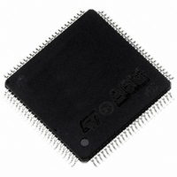
ST92F150CV1TB STMicroelectronics, ST92F150CV1TB Datasheet - Page 196

ST92F150CV1TB
Manufacturer Part Number
ST92F150CV1TB
Description
MCU 8BIT 128K FLASH 100TQFP
Manufacturer
STMicroelectronics
Series
ST9r
Datasheet
1.ST92F150CV1TB.pdf
(429 pages)
Specifications of ST92F150CV1TB
Core Processor
ST9
Core Size
8/16-Bit
Speed
24MHz
Connectivity
CAN, EBI/EMI, I²C, LIN, SCI, SPI
Peripherals
DMA, LVD, POR, PWM, WDT
Number Of I /o
77
Program Memory Size
128KB (128K x 8)
Program Memory Type
FLASH
Eeprom Size
1K x 8
Ram Size
4K x 8
Voltage - Supply (vcc/vdd)
4.5 V ~ 5.5 V
Data Converters
A/D 16x10b
Oscillator Type
Internal
Operating Temperature
-40°C ~ 105°C
Package / Case
100-TQFP, 100-VQFP
Processor Series
ST92F15x
Core
ST9
Data Bus Width
8 bit, 16 bit
Data Ram Size
6 KB
Interface Type
CAN, I2C, SCI, SPI
Maximum Clock Frequency
24 MHz
Number Of Programmable I/os
80
Number Of Timers
5 x 16 bit
Operating Supply Voltage
4.5 V to 5.5 V
Maximum Operating Temperature
+ 105 C
Mounting Style
SMD/SMT
Development Tools By Supplier
ST92F150-EPB
Minimum Operating Temperature
- 40 C
On-chip Adc
16 bit x 10 bit
Lead Free Status / RoHS Status
Lead free / RoHS Compliant
Other names
497-4883
Available stocks
Company
Part Number
Manufacturer
Quantity
Price
Company:
Part Number:
ST92F150CV1TB
Manufacturer:
STMicroelectronics
Quantity:
10 000
- Current page: 196 of 429
- Download datasheet (8Mb)
MULTIFUNCTION TIMER (MFT)
MULTIFUNCTION TIMER (Cont’d)
10.4.3.13 Autodiscrimination Mode
The phase between two pulses (respectively on in-
put pin B and input pin A) generates a one step up
(or down) count, so that the up/down control and
the counter clock are both external. Thus, if the ris-
ing edge of TxINB arrives when TxINA is at a low
level, the timer is incremented (no action if the ris-
ing edge of TxINB arrives when TxINA is at a high
level). If the falling edge of TxINB arrives when
TxINA is at a low level, the timer is decremented
(no action if the falling edge of TxINB arrives when
TxINA is at a high level).
Setting the UDC bit in the TCR register has no ef-
fect in this configuration.
10.4.3.14 TxINA = Trigger - TxINB = Ext. Clock
The signal applied to input pin A acts as a trigger
signal on REG0R, initiating the action for which the
register was programmed (i.e. a reload or cap-
196/429
9
ture), while the signal applied to input pin B is used
as the clock for the prescaler.
(*) The timer is in One shot mode and REG0R in
reload mode
10.4.3.15 TxINA = Ext. Clock - TxINB = Trigger
The signal applied to input pin B acts as a trigger,
performing a capture on REG1R, while the signal
applied to input pin A is used as the clock for the
prescaler.
10.4.3.16 TxINA = Trigger - TxINB = Gate
The signal applied to input pin A acts as a trigger
signal on REG0R, initiating the action for which the
register was programmed (i.e. a reload or cap-
ture), while the signal applied to input pin B acts as
a gate signal for the internal clock (i.e. the counter
runs only when the gate signal is at a low level).
Related parts for ST92F150CV1TB
Image
Part Number
Description
Manufacturer
Datasheet
Request
R

Part Number:
Description:
BOARD PROGRAM FOR ST92F150 MCU
Manufacturer:
STMicroelectronics
Datasheet:

Part Number:
Description:
BOARD EVALUATION FOR ST9 SERIES
Manufacturer:
STMicroelectronics
Datasheet:

Part Number:
Description:
BOARD EMULATOR FOR ST9 SERIES
Manufacturer:
STMicroelectronics
Datasheet:

Part Number:
Description:
MCU, MPU & DSP Development Tools ST9 Dedication Board
Manufacturer:
STMicroelectronics
Datasheet:

Part Number:
Description:
STMicroelectronics [RIPPLE-CARRY BINARY COUNTER/DIVIDERS]
Manufacturer:
STMicroelectronics
Datasheet:

Part Number:
Description:
STMicroelectronics [LIQUID-CRYSTAL DISPLAY DRIVERS]
Manufacturer:
STMicroelectronics
Datasheet:

Part Number:
Description:
BOARD EVAL FOR MEMS SENSORS
Manufacturer:
STMicroelectronics
Datasheet:

Part Number:
Description:
NPN TRANSISTOR POWER MODULE
Manufacturer:
STMicroelectronics
Datasheet:

Part Number:
Description:
TURBOSWITCH ULTRA-FAST HIGH VOLTAGE DIODE
Manufacturer:
STMicroelectronics
Datasheet:

Part Number:
Description:
Manufacturer:
STMicroelectronics
Datasheet:

Part Number:
Description:
DIODE / SCR MODULE
Manufacturer:
STMicroelectronics
Datasheet:

Part Number:
Description:
DIODE / SCR MODULE
Manufacturer:
STMicroelectronics
Datasheet:


