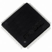
ST92F150CV1TB STMicroelectronics, ST92F150CV1TB Datasheet - Page 401

ST92F150CV1TB
Manufacturer Part Number
ST92F150CV1TB
Description
MCU 8BIT 128K FLASH 100TQFP
Manufacturer
STMicroelectronics
Series
ST9r
Datasheet
1.ST92F150CV1TB.pdf
(429 pages)
Specifications of ST92F150CV1TB
Core Processor
ST9
Core Size
8/16-Bit
Speed
24MHz
Connectivity
CAN, EBI/EMI, I²C, LIN, SCI, SPI
Peripherals
DMA, LVD, POR, PWM, WDT
Number Of I /o
77
Program Memory Size
128KB (128K x 8)
Program Memory Type
FLASH
Eeprom Size
1K x 8
Ram Size
4K x 8
Voltage - Supply (vcc/vdd)
4.5 V ~ 5.5 V
Data Converters
A/D 16x10b
Oscillator Type
Internal
Operating Temperature
-40°C ~ 105°C
Package / Case
100-TQFP, 100-VQFP
Processor Series
ST92F15x
Core
ST9
Data Bus Width
8 bit, 16 bit
Data Ram Size
6 KB
Interface Type
CAN, I2C, SCI, SPI
Maximum Clock Frequency
24 MHz
Number Of Programmable I/os
80
Number Of Timers
5 x 16 bit
Operating Supply Voltage
4.5 V to 5.5 V
Maximum Operating Temperature
+ 105 C
Mounting Style
SMD/SMT
Development Tools By Supplier
ST92F150-EPB
Minimum Operating Temperature
- 40 C
On-chip Adc
16 bit x 10 bit
Lead Free Status / RoHS Status
Lead free / RoHS Compliant
Other names
497-4883
Available stocks
Company
Part Number
Manufacturer
Quantity
Price
Company:
Part Number:
ST92F150CV1TB
Manufacturer:
STMicroelectronics
Quantity:
10 000
- Current page: 401 of 429
- Download datasheet (8Mb)
10-BIT ADC CHARACTERISTICS
Subject to general operating conditions for V
Figure 161. Typical Application with ADC
Notes:
1. Unless otherwise specified, typical data is based on T
guidelines and are not tested.
2. V
3. Any external serial impedance will downgrade the ADC accuracy (especially for resistance greater than 10 kΩ). Data
based on characterization results, not tested in production.
4. Value guaranteed by design.
Symbol
V
C
R
I
t
R
f
V
t
VDDA
STAB
ADC
ADC
AIN
AINx
ADC
ADC
AIN
AIN
may exceed A
ADC clock frequency
Conversion range voltage
Analog Input Voltage
External source impedance
Internal sample and hold capacitor
Analog input pin impedance
Stabilization time after ADC enable
Conversion time (Sample+Hold)
- Sample capacitor loading time
- Hold conversion time
VDDA input current
V
V
AIN
DD
VSS
Parameter
0.1
R
or A
AIN
μ
F
VDD
. However the conversion result in these cases will be 0000h or FFC0h respectively.
(2)
AINx
AV
AV
ST92F124/F150/F250 - ELECTRICAL CHARACTERISTICS
DD
SS
f
C
~2pF
ADC
DD
IO
, f
Conditions
= 4 MHz
A
OSC
=25°C and V
V
, and T
DD
A
DD
, unless otherwise specified.
-V
SS
=5V. These values are given only as design
AV
Min
-0.2
I
±1μA
1
7
LKADC
SS
Typ
6
1
20
(3,4)
8
(4)
1)
ADC
AV
10
AV
Max
DD
1.7
10
4
(3)
DD
+0.2
401/429
1/f
Unit
MHz
mA
kΩ
kΩ
pF
μs
V
ADC
1
Related parts for ST92F150CV1TB
Image
Part Number
Description
Manufacturer
Datasheet
Request
R

Part Number:
Description:
BOARD PROGRAM FOR ST92F150 MCU
Manufacturer:
STMicroelectronics
Datasheet:

Part Number:
Description:
BOARD EVALUATION FOR ST9 SERIES
Manufacturer:
STMicroelectronics
Datasheet:

Part Number:
Description:
BOARD EMULATOR FOR ST9 SERIES
Manufacturer:
STMicroelectronics
Datasheet:

Part Number:
Description:
MCU, MPU & DSP Development Tools ST9 Dedication Board
Manufacturer:
STMicroelectronics
Datasheet:

Part Number:
Description:
STMicroelectronics [RIPPLE-CARRY BINARY COUNTER/DIVIDERS]
Manufacturer:
STMicroelectronics
Datasheet:

Part Number:
Description:
STMicroelectronics [LIQUID-CRYSTAL DISPLAY DRIVERS]
Manufacturer:
STMicroelectronics
Datasheet:

Part Number:
Description:
BOARD EVAL FOR MEMS SENSORS
Manufacturer:
STMicroelectronics
Datasheet:

Part Number:
Description:
NPN TRANSISTOR POWER MODULE
Manufacturer:
STMicroelectronics
Datasheet:

Part Number:
Description:
TURBOSWITCH ULTRA-FAST HIGH VOLTAGE DIODE
Manufacturer:
STMicroelectronics
Datasheet:

Part Number:
Description:
Manufacturer:
STMicroelectronics
Datasheet:

Part Number:
Description:
DIODE / SCR MODULE
Manufacturer:
STMicroelectronics
Datasheet:

Part Number:
Description:
DIODE / SCR MODULE
Manufacturer:
STMicroelectronics
Datasheet:


