MCHC908QY1CDWE Freescale Semiconductor, MCHC908QY1CDWE Datasheet - Page 4
MCHC908QY1CDWE
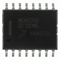
Manufacturer Part Number
MCHC908QY1CDWE
Description
IC MCU 1.5K FLASH 16-SOIC
Manufacturer
Freescale Semiconductor
Series
HC08r
Datasheet
1.MC908QY4MDWER.pdf
(184 pages)
Specifications of MCHC908QY1CDWE
Core Processor
HC08
Core Size
8-Bit
Speed
8MHz
Peripherals
LVD, POR, PWM
Number Of I /o
13
Program Memory Size
1.5KB (1.5K x 8)
Program Memory Type
FLASH
Ram Size
128 x 8
Voltage - Supply (vcc/vdd)
2.7 V ~ 5.5 V
Oscillator Type
Internal
Operating Temperature
-40°C ~ 85°C
Package / Case
16-SOIC (0.300", 7.5mm Width)
Processor Series
HC08QY
Core
HC08
Data Bus Width
8 bit
Data Ram Size
128 B
Maximum Clock Frequency
8 MHz
Number Of Programmable I/os
13
Number Of Timers
2
Maximum Operating Temperature
+ 85 C
Mounting Style
SMD/SMT
Development Tools By Supplier
FSICEBASE, M68CBL05AE, DEMO908QB8, DEMO908QC16
Minimum Operating Temperature
- 40 C
Lead Free Status / RoHS Status
Lead free / RoHS Compliant
Eeprom Size
-
Data Converters
-
Connectivity
-
Lead Free Status / Rohs Status
Details
Available stocks
Company
Part Number
Manufacturer
Quantity
Price
Company:

Part Number:
MCHC908QY1CDWE
Manufacturer:
Freescale
Quantity:
1 340
Part Number:
MCHC908QY1CDWE
Manufacturer:
FREESCALE
Quantity:
20 000


Revision History
The following revision history table summarizes changes contained in this document. For your
convenience, the page number designators have been linked to the appropriate location.
Revision History (Sheet 1 of 3)
4
September,
December,
January,
Date
2002
2002
2003
Revision
Level
N/A
0.1
0.2
Initial release
1.2 Features — Added 8-pin dual flat no lead (DFN) packages to features list.
Figure 1-2. MCU Pin Assignments — Figure updated to include DFN packages.
Figure 2-1. Memory Map — Clarified illegal address and unimplemented
memory.
Figure 2-2. Control, Status, and Data Registers — Corrected bit definitions for
Port A Data Register (PTA) and Data Direction Register A (DDRA).
Table 13-3. Interrupt Sources — Corrected vector addresses for keyboard
interrupt and ADC conversion complete interrupt.
Chapter 13 System Integration Module (SIM) — Removed reference to break
status register as it is duplicated in break module.
11.3.1 Internal Oscillator and 11.3.1.1 Internal Oscillator Trimming — Clarified
oscillator trim option ordering information and what to expect with untrimmed
device.
Figure 11-5. Oscillator Trim Register (OSCTRIM) — Bit 1 designation corrected.
Figure 15-13. Monitor Mode Circuit (Internal Clock, No High Voltage) —
Diagram updated for clarity.
Figure 12-1. I/O Port Register Summary — Corrected bit definitions for PTA7,
DDRA7, and DDRA6.
Figure 12-2. Port A Data Register (PTA) — Corrected bit definition for PTA7.
Figure 12-3. Data Direction Register A (DDRA) — Corrected bit definitions for
DDRA7 and DDRA6.
Figure 12-6. Port B Data Register (PTB) — Corrected bit definition for PTB1
Chapter 9 Keyboard Interrupt Module (KBI) — Section reworked after deletion
of auto wakeup for clarity.
Chapter 4 Auto Wakeup Module (AWU) — New section added for clarity.
Figure 10-1. LVI Module Block Diagram — Corrected LVI stop representation.
Chapter 16 Electrical Specifications — Extensive changes made to electrical
specifications.
17.5 8-Pin Dual Flat No Lead (DFN) Package (Case #1452) — Added case
outline drawing for DFN package.
Chapter 17 Ordering Information and Mechanical Specifications — Added
ordering information for DFN package.
4.2 Features — Corrected third bulleted item.
MC68HC908QY/QT Family Data Sheet, Rev. 6
Description
Freescale Semiconductor
Number(s)
Page
N/A
118
113
150
100
101
103
169
177
185
19
21
27
27
92
98
99
83
49
87
49
Related parts for MCHC908QY1CDWE
Image
Part Number
Description
Manufacturer
Datasheet
Request
R

Part Number:
Description:
Manufacturer:
Freescale Semiconductor, Inc
Datasheet:
Part Number:
Description:
Manufacturer:
Freescale Semiconductor, Inc
Datasheet:
Part Number:
Description:
Manufacturer:
Freescale Semiconductor, Inc
Datasheet:
Part Number:
Description:
Manufacturer:
Freescale Semiconductor, Inc
Datasheet:
Part Number:
Description:
Manufacturer:
Freescale Semiconductor, Inc
Datasheet:
Part Number:
Description:
Manufacturer:
Freescale Semiconductor, Inc
Datasheet:
Part Number:
Description:
Manufacturer:
Freescale Semiconductor, Inc
Datasheet:
Part Number:
Description:
Manufacturer:
Freescale Semiconductor, Inc
Datasheet:
Part Number:
Description:
Manufacturer:
Freescale Semiconductor, Inc
Datasheet:
Part Number:
Description:
Manufacturer:
Freescale Semiconductor, Inc
Datasheet:
Part Number:
Description:
Manufacturer:
Freescale Semiconductor, Inc
Datasheet:
Part Number:
Description:
Manufacturer:
Freescale Semiconductor, Inc
Datasheet:
Part Number:
Description:
Manufacturer:
Freescale Semiconductor, Inc
Datasheet:
Part Number:
Description:
Manufacturer:
Freescale Semiconductor, Inc
Datasheet:
Part Number:
Description:
Manufacturer:
Freescale Semiconductor, Inc
Datasheet: