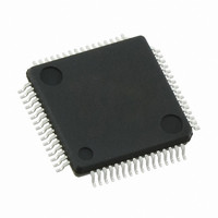
R5F212B7SNFP#U0 Renesas Electronics America, R5F212B7SNFP#U0 Datasheet - Page 481

R5F212B7SNFP#U0
Manufacturer Part Number
R5F212B7SNFP#U0
Description
IC R8C/2B MCU FLASH 64-LQFP
Manufacturer
Renesas Electronics America
Series
R8C/2x/2Br
Specifications of R5F212B7SNFP#U0
Core Processor
R8C
Core Size
16/32-Bit
Speed
20MHz
Connectivity
I²C, LIN, SIO, SSU, UART/USART
Peripherals
POR, PWM, Voltage Detect, WDT
Number Of I /o
55
Program Memory Size
48KB (48K x 8)
Program Memory Type
FLASH
Ram Size
2.5K x 8
Voltage - Supply (vcc/vdd)
2.2 V ~ 5.5 V
Data Converters
A/D 12x10b; D/A 2x8b
Oscillator Type
Internal
Operating Temperature
-20°C ~ 85°C
Package / Case
64-LQFP
For Use With
R0K5212D8S001BE - KIT STARTER FOR R8C/2DR0K5212D8S000BE - KIT DEV FOR R8C/2D
Lead Free Status / RoHS Status
Lead free / RoHS Compliant
Eeprom Size
-
Available stocks
Company
Part Number
Manufacturer
Quantity
Price
- Current page: 481 of 611
- Download datasheet (7Mb)
R8C/2A Group, R8C/2B Group
Rev.2.00
REJ09B0324-0200
17.3
Figure 17.2
LIN Control Register 2
LIN Control Register
The hardware LIN contains the registers listed below.
These registers are detailed in Figures 17.2 and 17.3.
b7 b6 b5
b7 b6 b5 b4
NOTES:
•
•
•
1.
2.
3. Inputs to timer RA and UART0 are prohibited immediately after this bit is set to 1. (Refer to Figure 17.5 Exam ple of
LIN Control Register 2 (LINCR2)
LIN Control Register (LINCR)
LIN Status Register (LINST)
Register Configuration
Nov 26, 2007
After setting the LSTART bit, confirm that the RXDSF flag is set to 1 before Synch Break input starts.
Before changing LIN operation modes, temporarily stop the LIN operation (LINE bit = 0).
Header Field Transm iss ion Flow chart (1) and Figure 17.9 Exam ple of Header Fie ld Re ception Flow chart
(2).)
b4
b3 b2 b1 b0
b3 b2 b1 b0
0 0
Registers LINCR2 and LINCR
Bit Symbol
Bit Symbol
(b2-b1)
(b7-b3)
LSTART
Symbol
LINCR2
Symbol
RXDSF
LINCR
BCE
SFIE
SBIE
BCIE
MST
SBE
LINE
Page 459 of 580
—
—
Bus collision during Sync Break
transmission detection enable bit
Reserved bits
Nothing is assigned. If necessary, set to 0.
When read, the content is 0.
Synch Field measurement-
completed interrupt enable bit
Synch Break detection interrupt
enable bit
Bus collision detection interrupt
enable bit
RXD0 input status flag
Synch Break detection start
bit(1)
RXD0 input unmasking timing
select bit (effective only in slave
mode)
LIN operation mode setting bit
LIN operation start bit
Address
Bit Name
0106h
Address
Bit Name
0105h
(2)
0 : Disables Synch Field measurement-
1 : Enables Synch Field measurement-
0 : Disables Synch Break detection interrupt
1 : Enables Synch Break detection interrupt
0 : Disables bus collision detection interrupt
1 : Enables bus collision detection interrupt
0 : RXD0 input enabled
1 : RXD0 input disabled
When this bit is set to 1, timer RA input is
enabled and RXD0 input is disabled.
When read, the content is 0.
0 : Unmasked after Synch Break is detected
1 : Unmasked after Synch Field measurement
0 : Slave mode
1 : Master mode
0 : Causes LIN to stop
1 : Causes LIN to start operating
completed interrupt
completed interrupt
is completed
(Synch Break detection circuit actuated)
(timer RA output OR’ed w ith TXD0)
0 : Disables bus collision detection
1 : Enables bus collision detection
Set to 0.
After Reset
Function
After Reset
Function
00h
00h
(3)
17. Hardware LIN
RW
RW
RW
RW
RW
RW
RW
RW
RW
RW
RW
RO
—
Related parts for R5F212B7SNFP#U0
Image
Part Number
Description
Manufacturer
Datasheet
Request
R

Part Number:
Description:
KIT STARTER FOR M16C/29
Manufacturer:
Renesas Electronics America
Datasheet:

Part Number:
Description:
KIT STARTER FOR R8C/2D
Manufacturer:
Renesas Electronics America
Datasheet:

Part Number:
Description:
R0K33062P STARTER KIT
Manufacturer:
Renesas Electronics America
Datasheet:

Part Number:
Description:
KIT STARTER FOR R8C/23 E8A
Manufacturer:
Renesas Electronics America
Datasheet:

Part Number:
Description:
KIT STARTER FOR R8C/25
Manufacturer:
Renesas Electronics America
Datasheet:

Part Number:
Description:
KIT STARTER H8S2456 SHARPE DSPLY
Manufacturer:
Renesas Electronics America
Datasheet:

Part Number:
Description:
KIT STARTER FOR R8C38C
Manufacturer:
Renesas Electronics America
Datasheet:

Part Number:
Description:
KIT STARTER FOR R8C35C
Manufacturer:
Renesas Electronics America
Datasheet:

Part Number:
Description:
KIT STARTER FOR R8CL3AC+LCD APPS
Manufacturer:
Renesas Electronics America
Datasheet:

Part Number:
Description:
KIT STARTER FOR RX610
Manufacturer:
Renesas Electronics America
Datasheet:

Part Number:
Description:
KIT STARTER FOR R32C/118
Manufacturer:
Renesas Electronics America
Datasheet:

Part Number:
Description:
KIT DEV RSK-R8C/26-29
Manufacturer:
Renesas Electronics America
Datasheet:

Part Number:
Description:
KIT STARTER FOR SH7124
Manufacturer:
Renesas Electronics America
Datasheet:

Part Number:
Description:
KIT STARTER FOR H8SX/1622
Manufacturer:
Renesas Electronics America
Datasheet:

Part Number:
Description:
KIT DEV FOR SH7203
Manufacturer:
Renesas Electronics America
Datasheet:


