R5F212B7SNFP#U0 Renesas Electronics America, R5F212B7SNFP#U0 Datasheet - Page 522
R5F212B7SNFP#U0
Manufacturer Part Number
R5F212B7SNFP#U0
Description
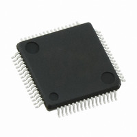
IC R8C/2B MCU FLASH 64-LQFP
Manufacturer
Renesas Electronics America
Series
R8C/2x/2Br
Specifications of R5F212B7SNFP#U0
Core Processor
R8C
Core Size
16/32-Bit
Speed
20MHz
Connectivity
I²C, LIN, SIO, SSU, UART/USART
Peripherals
POR, PWM, Voltage Detect, WDT
Number Of I /o
55
Program Memory Size
48KB (48K x 8)
Program Memory Type
FLASH
Ram Size
2.5K x 8
Voltage - Supply (vcc/vdd)
2.2 V ~ 5.5 V
Data Converters
A/D 12x10b; D/A 2x8b
Oscillator Type
Internal
Operating Temperature
-20°C ~ 85°C
Package / Case
64-LQFP
For Use With
R0K5212D8S001BE - KIT STARTER FOR R8C/2DR0K5212D8S000BE - KIT DEV FOR R8C/2D
Lead Free Status / RoHS Status
Lead free / RoHS Compliant
Eeprom Size
-
Available stocks
Company
Part Number
Manufacturer
Quantity
Price


R8C/2A Group, R8C/2B Group
Rev.2.00
REJ09B0324-0200
Figure 20.7
Flash Memory Control Register 4
b7 b6 b5 b4
NOTES:
1.
2.
3.
4.
5. Set the FMR01 bit in the FMR0 register to 0 (CPU rew rite mode disabled) in low -pow er consumption read mode.
0
To set this bit to 1, set it to 1 immediately after setting it first to 0. Do not generate an interrupt betw een setting the bit
to 0 and setting it to 1.
This bit is enabled w hen the FMR40 bit is set to 1 (enable) and it can be w ritten to during the period betw een issuing
an erase command and completing the erase. (This bit is set to 0 during periods other than above.)
In EW0 mode, it can be set to 0 or 1 by a program.
In EW1 mode, it is automatically set to 1 if a maskable interrupt is generated during an erase
operation w hile the FMR40 bit is set to 1. Do not set this bit to 1 by a program (0 can be w ritten).
The FMR42 bit is enabled only w hen the FMR40 bit is set to 1 (enable) and programming to the FMR42 bit is enabled
until auto-programming ends after a program command is generated. (This bit is set to 0 during periods other than the
above.)
In EW0 mode, 0 or 1 can be programmed to the FMR42 bit by a program.
In EW1 mode, the FMR42 bit is automatically set to 1 by generating a maskable interrupt during auto-programming
w hen the FMR40 bit is set to 1. 1 cannot be w ritten to the FMR42 bit by a program.
In high-speed clock mode and high-speed on-chip oscillator mode, set the FMR47 bit to 0 (disabled).
Nov 26, 2007
b3 b2
FMR4 Register
b1 b0
Bit Symbol
Symbol
FMR46
FMR47
FMR40
FMR41
FMR42
FMR43
FMR44
FMR4
(b5)
Page 500 of 580
—
Erase-suspend function
enable bit
Erase-suspend request bit
Program-suspend request bit
Erase command flag
Program command flag
Reserved bit
Read status flag
Low -pow er consumption read
mode enable bit
(1)
Address
Bit Name
01B3h
(1, 4, 5)
(2)
(3)
0 : Disable
1 : Enable
0 : Erase restart
1 : Erase-suspend request
0 : Program restart
1 : Program-suspend request
0 : Erase not executed
1 : Erase execution in progress
0 : Program not executed
1 : Program execution in progress
Set to 0.
0 : Disables reading
1 : Enables reading
0 : Disable
1 : Enable
After Reset
01000000b
Function
20. Flash Memory
RW
RW
RW
RW
RW
RO
RO
RO
RO
Related parts for R5F212B7SNFP#U0
Image
Part Number
Description
Manufacturer
Datasheet
Request
R

Part Number:
Description:
KIT STARTER FOR M16C/29
Manufacturer:
Renesas Electronics America
Datasheet:

Part Number:
Description:
KIT STARTER FOR R8C/2D
Manufacturer:
Renesas Electronics America
Datasheet:

Part Number:
Description:
R0K33062P STARTER KIT
Manufacturer:
Renesas Electronics America
Datasheet:

Part Number:
Description:
KIT STARTER FOR R8C/23 E8A
Manufacturer:
Renesas Electronics America
Datasheet:

Part Number:
Description:
KIT STARTER FOR R8C/25
Manufacturer:
Renesas Electronics America
Datasheet:

Part Number:
Description:
KIT STARTER H8S2456 SHARPE DSPLY
Manufacturer:
Renesas Electronics America
Datasheet:

Part Number:
Description:
KIT STARTER FOR R8C38C
Manufacturer:
Renesas Electronics America
Datasheet:

Part Number:
Description:
KIT STARTER FOR R8C35C
Manufacturer:
Renesas Electronics America
Datasheet:

Part Number:
Description:
KIT STARTER FOR R8CL3AC+LCD APPS
Manufacturer:
Renesas Electronics America
Datasheet:
Part Number:
Description:
KIT STARTER FOR RX610
Manufacturer:
Renesas Electronics America
Datasheet:

Part Number:
Description:
KIT STARTER FOR R32C/118
Manufacturer:
Renesas Electronics America
Datasheet:

Part Number:
Description:
KIT DEV RSK-R8C/26-29
Manufacturer:
Renesas Electronics America
Datasheet:

Part Number:
Description:
KIT STARTER FOR SH7124
Manufacturer:
Renesas Electronics America
Datasheet:

Part Number:
Description:
KIT STARTER FOR H8SX/1622
Manufacturer:
Renesas Electronics America
Datasheet:

Part Number:
Description:
KIT DEV FOR SH7203
Manufacturer:
Renesas Electronics America
Datasheet: