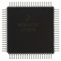
MC9S12C32CFUE16 Freescale Semiconductor, MC9S12C32CFUE16 Datasheet - Page 213

MC9S12C32CFUE16
Manufacturer Part Number
MC9S12C32CFUE16
Description
IC MCU 32K FLASH 16MHZ 80-QFP
Manufacturer
Freescale Semiconductor
Series
HCS12r
Datasheets
1.MC9S12GC16MFUE.pdf
(690 pages)
2.MC9S12C96CFUER.pdf
(26 pages)
3.MC9S12C32CFAE25.pdf
(2 pages)
Specifications of MC9S12C32CFUE16
Core Processor
HCS12
Core Size
16-Bit
Speed
16MHz
Connectivity
CAN, EBI/EMI, SCI, SPI
Peripherals
POR, PWM, WDT
Number Of I /o
60
Program Memory Size
32KB (32K x 8)
Program Memory Type
FLASH
Ram Size
2K x 8
Voltage - Supply (vcc/vdd)
2.35 V ~ 5.5 V
Data Converters
A/D 8x10b
Oscillator Type
Internal
Operating Temperature
-40°C ~ 85°C
Package / Case
80-QFP
Processor Series
S12C
Core
HCS12
Data Bus Width
16 bit
Data Ram Size
2 KB
Interface Type
CAN/SCI/SPI
Maximum Clock Frequency
16 MHz
Number Of Programmable I/os
60
Number Of Timers
8
Operating Supply Voltage
- 0.3 V to + 6.5 V
Maximum Operating Temperature
+ 85 C
Mounting Style
SMD/SMT
3rd Party Development Tools
EWHCS12
Development Tools By Supplier
M68EVB912C32EE
Minimum Operating Temperature
- 40 C
On-chip Adc
8-ch x 10-bit
For Use With
CML12C32SLK - KIT STUDENT LEARNING 16BIT HCS12
Lead Free Status / RoHS Status
Lead free / RoHS Compliant
Eeprom Size
-
Lead Free Status / Rohs Status
Lead free / RoHS Compliant
Available stocks
Company
Part Number
Manufacturer
Quantity
Price
Company:
Part Number:
MC9S12C32CFUE16
Manufacturer:
Freescale Semiconductor
Quantity:
10 000
- Current page: 213 of 690
- Download datasheet (4Mb)
DBGC2 being logic 1 or logic 0, respectively. BDM requests have a higher priority than SWI requests. No
data breakpoints are allowed in this mode.
TAGAB in DBGC2 selects whether the breakpoint mode is forced or tagged. The BKxMBH:L bits in
DBGC3 select whether or not the breakpoint is matched exactly or is a range breakpoint. They also select
whether the address is matched on the high byte, low byte, both bytes, and/or memory expansion. The
RWx and RWxEN bits in DBGC3 select whether the type of bus cycle to match is a read, write, or
read/write when performing forced breakpoints.
7.4.1.2
Full breakpoint mode requires a match on address and data for a breakpoint to occur. Upon a successful
match, the system will enter background debug mode or initiate a software interrupt based upon the state
of BDM in DBGC2 being logic 1 or logic 0, respectively. BDM requests have a higher priority than SWI
requests. R/W matches are also allowed in this mode.
TAGAB in DBGC2 selects whether the breakpoint mode is forced or tagged. When TAGAB is set in
DBGC2, only addresses are compared and data is ignored. The BKAMBH:L bits in DBGC3 select
whether or not the breakpoint is matched exactly, is a range breakpoint, or is in page space. The
BKBMBH:L bits in DBGC3 select whether the data is matched on the high byte, low byte, or both bytes.
RWA and RWAEN bits in DBGC2 select whether the type of bus cycle to match is a read or a write when
performing forced breakpoints. RWB and RWBEN bits in DBGC2 are not used in full breakpoint mode.
7.4.1.3
Breakpoint operation is first determined by the state of the BDM module. If the BDM module is already
active, meaning the CPU is executing out of BDM firmware, breakpoints are not allowed. In addition,
while executing a BDM TRACE command, tagging into BDM is not allowed. If BDM is not active, the
breakpoint will give priority to BDM requests over SWI requests. This condition applies to both forced
and tagged breakpoints.
In all cases, BDM related breakpoints will have priority over those generated by the Breakpoint sub-block.
This priority includes breakpoints enabled by the TAGLO and TAGHI external pins of the system that
interface with the BDM directly and whose signal information passes through and is used by the
breakpoint sub-block.
Freescale Semiconductor
Full Breakpoint Mode
Breakpoint Priority
The full trigger mode is designed to be used for either a word access or a
byte access, but not both at the same time. Confusing trigger operation
(seemingly false triggers or no trigger) can occur if the trigger address
occurs in the user program as both byte and word accesses.
MC9S12C-Family / MC9S12GC-Family
Rev 01.24
NOTE
Chapter 7 Debug Module (DBGV1) Block Description
213
Related parts for MC9S12C32CFUE16
Image
Part Number
Description
Manufacturer
Datasheet
Request
R
Part Number:
Description:
Manufacturer:
Freescale Semiconductor, Inc
Datasheet:
Part Number:
Description:
Manufacturer:
Freescale Semiconductor, Inc
Datasheet:
Part Number:
Description:
Manufacturer:
Freescale Semiconductor, Inc
Datasheet:
Part Number:
Description:
Manufacturer:
Freescale Semiconductor, Inc
Datasheet:
Part Number:
Description:
Manufacturer:
Freescale Semiconductor, Inc
Datasheet:
Part Number:
Description:
Manufacturer:
Freescale Semiconductor, Inc
Datasheet:
Part Number:
Description:
Manufacturer:
Freescale Semiconductor, Inc
Datasheet:
Part Number:
Description:
Manufacturer:
Freescale Semiconductor, Inc
Datasheet:
Part Number:
Description:
Manufacturer:
Freescale Semiconductor, Inc
Datasheet:
Part Number:
Description:
Manufacturer:
Freescale Semiconductor, Inc
Datasheet:
Part Number:
Description:
Manufacturer:
Freescale Semiconductor, Inc
Datasheet:
Part Number:
Description:
Manufacturer:
Freescale Semiconductor, Inc
Datasheet:
Part Number:
Description:
Manufacturer:
Freescale Semiconductor, Inc
Datasheet:
Part Number:
Description:
Manufacturer:
Freescale Semiconductor, Inc
Datasheet:
Part Number:
Description:
Manufacturer:
Freescale Semiconductor, Inc
Datasheet:


