MC9S12C32CFUE16 Freescale Semiconductor, MC9S12C32CFUE16 Datasheet - Page 266
MC9S12C32CFUE16
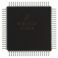
Manufacturer Part Number
MC9S12C32CFUE16
Description
IC MCU 32K FLASH 16MHZ 80-QFP
Manufacturer
Freescale Semiconductor
Series
HCS12r
Datasheets
1.MC9S12GC16MFUE.pdf
(690 pages)
2.MC9S12C96CFUER.pdf
(26 pages)
3.MC9S12C32CFAE25.pdf
(2 pages)
Specifications of MC9S12C32CFUE16
Core Processor
HCS12
Core Size
16-Bit
Speed
16MHz
Connectivity
CAN, EBI/EMI, SCI, SPI
Peripherals
POR, PWM, WDT
Number Of I /o
60
Program Memory Size
32KB (32K x 8)
Program Memory Type
FLASH
Ram Size
2K x 8
Voltage - Supply (vcc/vdd)
2.35 V ~ 5.5 V
Data Converters
A/D 8x10b
Oscillator Type
Internal
Operating Temperature
-40°C ~ 85°C
Package / Case
80-QFP
Processor Series
S12C
Core
HCS12
Data Bus Width
16 bit
Data Ram Size
2 KB
Interface Type
CAN/SCI/SPI
Maximum Clock Frequency
16 MHz
Number Of Programmable I/os
60
Number Of Timers
8
Operating Supply Voltage
- 0.3 V to + 6.5 V
Maximum Operating Temperature
+ 85 C
Mounting Style
SMD/SMT
3rd Party Development Tools
EWHCS12
Development Tools By Supplier
M68EVB912C32EE
Minimum Operating Temperature
- 40 C
On-chip Adc
8-ch x 10-bit
For Use With
CML12C32SLK - KIT STUDENT LEARNING 16BIT HCS12
Lead Free Status / RoHS Status
Lead free / RoHS Compliant
Eeprom Size
-
Lead Free Status / Rohs Status
Lead free / RoHS Compliant
Available stocks
Company
Part Number
Manufacturer
Quantity
Price

Company:
Part Number:
MC9S12C32CFUE16
Manufacturer:
Freescale Semiconductor
Quantity:
10 000


Chapter 9 Clocks and Reset Generator (CRGV4) Block Description
9.3.2.12
This register is used to restart the COP time-out period.
Read: always reads 0x0000
Write: anytime
When the COP is disabled (CR[2:0] = “000”) writing to this register has no effect.
When the COP is enabled by setting CR[2:0] nonzero, the following applies:
9.4
This section gives detailed informations on the internal operation of the design.
9.4.1
The PLL is used to run the MCU from a different time base than the incoming OSCCLK. For increased
flexibility, OSCCLK can be divided in a range of 1 to 16 to generate the reference frequency. This offers
a finer multiplication granularity. The PLL can multiply this reference clock by a multiple of 2, 4, 6,...
126,128 based on the SYNR register.
266
Module Base + 0x000B
Reset
W
R
Writing any value other than 0x0055 or 0x00AA causes a COP reset. To restart the COP time-out
period you must write 0x0055 followed by a write of 0x00AA. Other instructions may be executed
between these writes but the sequence (0x0055, 0x00AA) must be completed prior to COP end of
time-out period to avoid a COP reset. Sequences of 0x0055 writes or sequences of 0x00AA writes
are allowed. When the WCOP bit is set, 0x0055 and 0x00AA writes must be done in the last 25%
of the selected time-out period; writing any value in the first 75% of the selected period will cause
a COP reset.
Functional Description
Phase Locked Loop (PLL)
Bit 7
CRG COP Timer Arm/Reset Register (ARMCOP)
0
0
7
Although it is possible to set the two dividers to command a very high clock
frequency, do not exceed the specified bus frequency limit for the MCU.
If (PLLSEL = 1), Bus Clock = PLLCLK / 2
Bit 6
0
0
6
Figure 9-15. ARMCOP Register Diagram
PLLCLK
MC9S12C-Family / MC9S12GC-Family
Bit 5
0
0
5
=
2 OSCCLK
×
CAUTION
Rev 01.24
Bit 4
0
0
4
×
--------------------------------- -
[
[
REFDV
SYNR
Bit 3
0
0
3
+
+
1
1
]
]
Bit 2
0
0
2
Freescale Semiconductor
Bit 1
0
0
1
Bit 0
0
0
0
Related parts for MC9S12C32CFUE16
Image
Part Number
Description
Manufacturer
Datasheet
Request
R

Part Number:
Description:
Manufacturer:
Freescale Semiconductor, Inc
Datasheet:
Part Number:
Description:
Manufacturer:
Freescale Semiconductor, Inc
Datasheet:
Part Number:
Description:
Manufacturer:
Freescale Semiconductor, Inc
Datasheet:
Part Number:
Description:
Manufacturer:
Freescale Semiconductor, Inc
Datasheet:
Part Number:
Description:
Manufacturer:
Freescale Semiconductor, Inc
Datasheet:
Part Number:
Description:
Manufacturer:
Freescale Semiconductor, Inc
Datasheet:
Part Number:
Description:
Manufacturer:
Freescale Semiconductor, Inc
Datasheet:
Part Number:
Description:
Manufacturer:
Freescale Semiconductor, Inc
Datasheet:
Part Number:
Description:
Manufacturer:
Freescale Semiconductor, Inc
Datasheet:
Part Number:
Description:
Manufacturer:
Freescale Semiconductor, Inc
Datasheet:
Part Number:
Description:
Manufacturer:
Freescale Semiconductor, Inc
Datasheet:
Part Number:
Description:
Manufacturer:
Freescale Semiconductor, Inc
Datasheet:
Part Number:
Description:
Manufacturer:
Freescale Semiconductor, Inc
Datasheet:
Part Number:
Description:
Manufacturer:
Freescale Semiconductor, Inc
Datasheet:
Part Number:
Description:
Manufacturer:
Freescale Semiconductor, Inc
Datasheet: