SAF-C164CI-8EM CB Infineon Technologies, SAF-C164CI-8EM CB Datasheet - Page 54
SAF-C164CI-8EM CB
Manufacturer Part Number
SAF-C164CI-8EM CB
Description
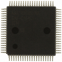
IC MCU 16BIT OTP MQFP-80-1
Manufacturer
Infineon Technologies
Series
C16xxr
Datasheet
1.SAF-C164CI-8EM_CB.pdf
(79 pages)
Specifications of SAF-C164CI-8EM CB
Core Processor
C166
Core Size
16-Bit
Speed
20MHz
Connectivity
CAN, EBI/EMI, SPI, SSC, UART/USART
Peripherals
POR, PWM, WDT
Number Of I /o
59
Program Memory Size
64KB (64K x 8)
Program Memory Type
OTP
Ram Size
4K x 8
Voltage - Supply (vcc/vdd)
4.75 V ~ 5.5 V
Data Converters
A/D 8x10b
Oscillator Type
External
Operating Temperature
-40°C ~ 85°C
Package / Case
80-SQFP
Data Bus Width
16 bit
Data Ram Size
4 KB
Interface Type
ASC, CAN, SSC
Maximum Clock Frequency
20 MHz
Number Of Programmable I/os
59
Number Of Timers
3
Maximum Operating Temperature
+ 85 C
Mounting Style
SMD/SMT
Minimum Operating Temperature
- 40 C
On-chip Adc
10 bit, 8 Channel
Packages
PG-MQFP-80
Max Clock Frequency
20.0 MHz
Sram (incl. Cache)
4.0 KByte
Can Nodes
1
A / D Input Lines (incl. Fadc)
8
Program Memory
64.0 KByte
Lead Free Status / RoHS Status
Lead free / RoHS Compliant
Eeprom Size
-
Lead Free Status / Rohs Status
Details
Other names
F164CI8EMCBNT
F164CI8EMCBXT
SAF-C164CI-8EMCB
SAF-C164CI-8EMCBINTR
SAF-C164CI-8EMCBTR
SAF-C164CI-8EMCBTR
SAFC164CI8EMCBXT
SP000103499
F164CI8EMCBXT
SAF-C164CI-8EMCB
SAF-C164CI-8EMCBINTR
SAF-C164CI-8EMCBTR
SAF-C164CI-8EMCBTR
SAFC164CI8EMCBXT
SP000103499


AC Characteristics
Definition of Internal Timing
The internal operation of the C164CI is controlled by the internal CPU clock
edges of the CPU clock can trigger internal (e.g. pipeline) or external (e.g. bus cycles)
operations.
The specification of the external timing (AC Characteristics) therefore depends on the
time between two consecutive edges of the CPU clock, called “TCL” (see
Figure 11
The CPU clock signal
different mechanisms. The duration of TCLs and their variation (and also the derived
external timing) depends on the used mechanism to generate
be regarded when calculating the timings for the C164CI.
Note: The example for PLL operation shown in
The used mechanism to generate the basic CPU clock is selected by bitfield CLKCFG
in register RP0H.7-5.
Upon a long hardware reset register RP0H is loaded with the logic levels present on the
upper half of PORT0 (P0H), i.e. bitfield CLKCFG represents the logic levels on pins
Data Sheet
Phase Locked Loop Operation
f
f
Direct Clock Drive
f
f
Prescaler Operation
f
f
OSC
CPU
OSC
CPU
OSC
CPU
Generation Mechanisms for the CPU Clock
f
CPU
can be generated from the oscillator clock signal
50
Figure 11
refers to a PLL factor of 4.
TCL
f
CPU
TCL
. This influence must
TCL
TCL
TCL
TCL
MCT04338
Figure
C164CL/SL
V2.0, 2001-05
C164CI/SI
f
CPU
f
OSC
. Both
11).
via
Related parts for SAF-C164CI-8EM CB
Image
Part Number
Description
Manufacturer
Datasheet
Request
R

Part Number:
Description:
SAF-C164CI-LM16-Bit Single-Chip Microcontroller
Manufacturer:
Infineon Technologies AG
Datasheet:
Part Number:
Description:
Manufacturer:
Infineon Technologies AG
Datasheet:
Part Number:
Description:
MQFP 80/ 16 BIT MCU 64 K OTP, 4 K RAM, CAN, DRIVE CONTROL UNIT, ENH. POWER
Manufacturer:
Infineon Technologies AG
Datasheet:
Part Number:
Description:
Manufacturer:
Infineon Technologies AG
Datasheet:

Part Number:
Description:
IC MCU 16BIT 64KB OTP MQFP-80-1
Manufacturer:
Infineon Technologies
Datasheet:

Part Number:
Description:
IC MCU 16BIT FLASH 80-MQFP
Manufacturer:
Infineon Technologies
Datasheet:
Part Number:
Description:
IC MCU 16BIT OTP MQFP-80-1
Manufacturer:
Infineon Technologies
Datasheet:
Part Number:
Description:
IC MCU 16BIT OTP MQFP-80-1
Manufacturer:
Infineon Technologies
Datasheet:
Part Number:
Description:
IC MCU 16BIT OTP MQFP-80-1
Manufacturer:
Infineon Technologies
Datasheet:
Part Number:
Description:
16-bit Microcontrollers - MCU
Manufacturer:
Infineon Technologies
Part Number:
Description:
Manufacturer:
Infineon Technologies AG
Datasheet:
Part Number:
Description:
Manufacturer:
Infineon Technologies AG
Datasheet:
Part Number:
Description:
Manufacturer:
Infineon Technologies AG
Datasheet: