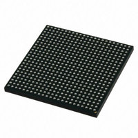
MCIMX512DJM8C Freescale Semiconductor, MCIMX512DJM8C Datasheet - Page 136

MCIMX512DJM8C
Manufacturer Part Number
MCIMX512DJM8C
Description
MULTIMEDIA PROC 529-LFBGA
Manufacturer
Freescale Semiconductor
Series
i.MX51r
Specifications of MCIMX512DJM8C
Core Processor
ARM Cortex-A8
Core Size
32-Bit
Speed
800MHz
Connectivity
1-Wire, EBI/EMI, Ethernet, I²C, IrDA, MMC, SPI, SSI, UART/USART, USB OTG
Peripherals
DMA, I²S, LCD, POR, PWM, WDT
Number Of I /o
128
Program Memory Type
ROMless
Ram Size
128K x 8
Voltage - Supply (vcc/vdd)
0.8 V ~ 1.15 V
Oscillator Type
External
Operating Temperature
-20°C ~ 85°C
Package / Case
529-LFBGA
Processor Series
i.MX51
Core
ARM Cortex A8
Data Bus Width
32 bit
Program Memory Size
36 KB
Data Ram Size
128 KB
Interface Type
I2C, SPI, SSI, UART, USB
Maximum Clock Frequency
200 MHz
Number Of Timers
5
Operating Supply Voltage
0.8 V to 1.15 V
Maximum Operating Temperature
+ 85 C
Mounting Style
SMD/SMT
3rd Party Development Tools
MDK-ARM, RL-ARM, ULINK2
Development Tools By Supplier
MCIMX51EVKJ
Minimum Operating Temperature
- 20 C
Lead Free Status / RoHS Status
Lead free / RoHS Compliant
Eeprom Size
-
Program Memory Size
-
Data Converters
-
Lead Free Status / Rohs Status
Lead free / RoHS Compliant
Available stocks
Company
Part Number
Manufacturer
Quantity
Price
Company:
Part Number:
MCIMX512DJM8C
Manufacturer:
Freescale Semiconductor
Quantity:
10 000
Part Number:
MCIMX512DJM8C
Manufacturer:
FREESCALE
Quantity:
20 000
- Current page: 136 of 200
- Download datasheet (6Mb)
Electrical Characteristics
136
SS39
SS44
SS45
SS46
ID
(Tx) CK high to STXD high impedance
SRXD setup before (Tx) CK falling
SRXD hold after (Tx) CK falling
SRXD rise/fall time
•
•
•
•
•
i.MX51 Applications Processors for Consumer and Industrial Products, Rev. 4
All the timings for the SSI are given for a non-inverted serial clock
polarity (TSCKP/RSCKP = 0) and a non-inverted frame sync
(TFSI/RFSI = 0). If the polarity of the clock and/or the frame sync have
been inverted, all the timing remains valid by inverting the clock signal
STCK/SRCK and/or the frame sync STFS/SRFS shown in the tables
and in the figures.
All timings are on Audiomux Pads when SSI is being used for data
transfer.
“Tx” and “Rx” refer to the Transmit and Receive sections of the SSI.
The terms WL and BL refer to Word Length (WL) and Bit Length (BL).
For internal Frame Sync operation using external clock, the FS timing is
same as that of Tx Data (for example, during AC97 mode of operation).
Table 104. SSI Transmitter Timing with External Clock (continued)
Parameter
Synchronous External Clock Operation
NOTE
10.0
Min
2.0
—
—
Freescale Semiconductor
Max
15.0
6.0
—
—
Unit
ns
ns
ns
ns
Related parts for MCIMX512DJM8C
Image
Part Number
Description
Manufacturer
Datasheet
Request
R
Part Number:
Description:
MCIMX-LVDS1
Manufacturer:
Freescale Semiconductor
Datasheet:
Part Number:
Description:
Manufacturer:
Freescale Semiconductor, Inc
Datasheet:
Part Number:
Description:
Manufacturer:
Freescale Semiconductor, Inc
Datasheet:
Part Number:
Description:
Manufacturer:
Freescale Semiconductor, Inc
Datasheet:
Part Number:
Description:
Manufacturer:
Freescale Semiconductor, Inc
Datasheet:
Part Number:
Description:
Manufacturer:
Freescale Semiconductor, Inc
Datasheet:
Part Number:
Description:
Manufacturer:
Freescale Semiconductor, Inc
Datasheet:
Part Number:
Description:
Manufacturer:
Freescale Semiconductor, Inc
Datasheet:
Part Number:
Description:
Manufacturer:
Freescale Semiconductor, Inc
Datasheet:
Part Number:
Description:
Manufacturer:
Freescale Semiconductor, Inc
Datasheet:
Part Number:
Description:
Manufacturer:
Freescale Semiconductor, Inc
Datasheet:
Part Number:
Description:
Manufacturer:
Freescale Semiconductor, Inc
Datasheet:
Part Number:
Description:
Manufacturer:
Freescale Semiconductor, Inc
Datasheet:
Part Number:
Description:
Manufacturer:
Freescale Semiconductor, Inc
Datasheet:
Part Number:
Description:
Manufacturer:
Freescale Semiconductor, Inc
Datasheet:


