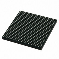
MCIMX512DJM8C Freescale Semiconductor, MCIMX512DJM8C Datasheet - Page 46

MCIMX512DJM8C
Manufacturer Part Number
MCIMX512DJM8C
Description
MULTIMEDIA PROC 529-LFBGA
Manufacturer
Freescale Semiconductor
Series
i.MX51r
Specifications of MCIMX512DJM8C
Core Processor
ARM Cortex-A8
Core Size
32-Bit
Speed
800MHz
Connectivity
1-Wire, EBI/EMI, Ethernet, I²C, IrDA, MMC, SPI, SSI, UART/USART, USB OTG
Peripherals
DMA, I²S, LCD, POR, PWM, WDT
Number Of I /o
128
Program Memory Type
ROMless
Ram Size
128K x 8
Voltage - Supply (vcc/vdd)
0.8 V ~ 1.15 V
Oscillator Type
External
Operating Temperature
-20°C ~ 85°C
Package / Case
529-LFBGA
Processor Series
i.MX51
Core
ARM Cortex A8
Data Bus Width
32 bit
Program Memory Size
36 KB
Data Ram Size
128 KB
Interface Type
I2C, SPI, SSI, UART, USB
Maximum Clock Frequency
200 MHz
Number Of Timers
5
Operating Supply Voltage
0.8 V to 1.15 V
Maximum Operating Temperature
+ 85 C
Mounting Style
SMD/SMT
3rd Party Development Tools
MDK-ARM, RL-ARM, ULINK2
Development Tools By Supplier
MCIMX51EVKJ
Minimum Operating Temperature
- 20 C
Lead Free Status / RoHS Status
Lead free / RoHS Compliant
Eeprom Size
-
Program Memory Size
-
Data Converters
-
Lead Free Status / Rohs Status
Lead free / RoHS Compliant
Available stocks
Company
Part Number
Manufacturer
Quantity
Price
Company:
Part Number:
MCIMX512DJM8C
Manufacturer:
Freescale Semiconductor
Quantity:
10 000
Part Number:
MCIMX512DJM8C
Manufacturer:
FREESCALE
Quantity:
20 000
- Current page: 46 of 200
- Download datasheet (6Mb)
Electrical Characteristics
4.6
This section contains the timing and electrical parameters for the modules in the i.MX51 processor.
4.6.1
Figure 12
46
1
2
3
Output Pad di/dt (Low drive)
Input Pad Transition Times
Input Pad Propagation Delay (DDR input),
50%-50%
Maximum Input Transition Times
Max condition for tpr, tpo, tps and didt: wcs model, 1.1 V, IO 1.65 V, 105 °C and s0-s5=111111. Typ condition for tpr, tpo,
tps and didt: typ model, 1.2 V, IO 1.8 V, 25 °C and s0-s5=101010. Min condition for tpr, tpo, tps and didt: bcs model, 1.3 V,
IO 1.95 V, –40 °C and s0-s5=000000.
Max condition for trfi and tpi: wcs model, 1.1 V, IO 1.65 V and 105 °C. Typ condition for trfi and tpi: typ model, 1.2 V, IO
1.8 V and 25 °C. Min condition for trfi and tpi: bcs model, 1.3 V, IO 1.95 V and –40 °C.
Hysteresis mode is recommended for input with transition time greater than 25 ns.
CC1
ID
Module Timing
shows the reset timing and
2
Duration of RESET_IN to be qualified as valid (input slope = 5 ns)
Reset Timings Parameters
Table 44. AC Electrical Characteristics of DDR mobile IO Pads for Slow Mode and
i.MX51 Applications Processors for Consumer and Industrial Products, Rev. 4
Parameter
RESET_IN
(Input)
2
1
3
ovdd=1.65 – 1.95 V (ipp_hve=0) (continued)
Table 45. Reset Timing Parameters
Figure 12. Reset Timing Diagram
Parameter
Table 45
Symbol
lists the timing parameters.
di/dt
trm
trfi
tpi
Condition
CC1
1.2 pF
1.2 pF
Test
—
—
0.09/0.09 0.132/0.128 0.212/0.213
0.3/0.36
rise/fall
Min
12
—
0.5/0.52
Min
50
Typ
—
5
Freescale Semiconductor
0.82/0.94
rise/fall
Max
—
Max
3
5
mA/ns
Units
Unit
ns
ns
ns
—
Related parts for MCIMX512DJM8C
Image
Part Number
Description
Manufacturer
Datasheet
Request
R
Part Number:
Description:
MCIMX-LVDS1
Manufacturer:
Freescale Semiconductor
Datasheet:
Part Number:
Description:
Manufacturer:
Freescale Semiconductor, Inc
Datasheet:
Part Number:
Description:
Manufacturer:
Freescale Semiconductor, Inc
Datasheet:
Part Number:
Description:
Manufacturer:
Freescale Semiconductor, Inc
Datasheet:
Part Number:
Description:
Manufacturer:
Freescale Semiconductor, Inc
Datasheet:
Part Number:
Description:
Manufacturer:
Freescale Semiconductor, Inc
Datasheet:
Part Number:
Description:
Manufacturer:
Freescale Semiconductor, Inc
Datasheet:
Part Number:
Description:
Manufacturer:
Freescale Semiconductor, Inc
Datasheet:
Part Number:
Description:
Manufacturer:
Freescale Semiconductor, Inc
Datasheet:
Part Number:
Description:
Manufacturer:
Freescale Semiconductor, Inc
Datasheet:
Part Number:
Description:
Manufacturer:
Freescale Semiconductor, Inc
Datasheet:
Part Number:
Description:
Manufacturer:
Freescale Semiconductor, Inc
Datasheet:
Part Number:
Description:
Manufacturer:
Freescale Semiconductor, Inc
Datasheet:
Part Number:
Description:
Manufacturer:
Freescale Semiconductor, Inc
Datasheet:
Part Number:
Description:
Manufacturer:
Freescale Semiconductor, Inc
Datasheet:


