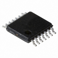
P87LPC760BDH,112 NXP Semiconductors, P87LPC760BDH,112 Datasheet - Page 11

P87LPC760BDH,112
Manufacturer Part Number
P87LPC760BDH,112
Description
IC 80C51 MCU 1K OTP 14-TSSOP
Manufacturer
NXP Semiconductors
Series
LPC700r
Datasheet
1.P87LPC760BN112.pdf
(56 pages)
Specifications of P87LPC760BDH,112
Program Memory Type
OTP
Program Memory Size
1KB (1K x 8)
Package / Case
14-TSSOP
Core Processor
8051
Core Size
8-Bit
Speed
20MHz
Connectivity
I²C, UART/USART
Peripherals
Brown-out Detect/Reset, LED, POR, WDT
Number Of I /o
12
Ram Size
128 x 8
Voltage - Supply (vcc/vdd)
2.7 V ~ 6 V
Oscillator Type
Internal
Operating Temperature
0°C ~ 70°C
Processor Series
P87LPC7x
Core
80C51
Data Bus Width
8 bit
Data Ram Size
128 B
Interface Type
I2C/UART
Maximum Clock Frequency
20 MHz
Number Of Programmable I/os
12
Number Of Timers
2
Operating Supply Voltage
2.7 V to 6 V
Maximum Operating Temperature
+ 70 C
Mounting Style
SMD/SMT
3rd Party Development Tools
PK51, CA51, A51, ULINK2
Minimum Operating Temperature
0 C
Lead Free Status / RoHS Status
Lead free / RoHS Compliant
For Use With
OM10063 - PROGRAMMER LPC700 P76XLCPOM10050 - EMULATOR LPC700 PDS76X
Eeprom Size
-
Data Converters
-
Lead Free Status / Rohs Status
Lead free / RoHS Compliant
Other names
568-1015-5
935271146112
P87LPC760BDH
935271146112
P87LPC760BDH
Philips Semiconductors
FUNCTIONAL DESCRIPTION
Details of P87LPC760 functions will be described in the following
sections.
Enhanced CPU
The P87LPC760 uses an enhanced 80C51 CPU which runs at twice
the speed of standard 80C51 devices. This means that the
performance of the P87LPC760 running at 5 MHz is exactly the
same as that of a standard 80C51 running at 10 MHz. A machine
cycle consists of 6 oscillator cycles, and most instructions execute in
6 or 12 clocks. A user configurable option allows restoring standard
80C51 execution timing. In that case, a machine cycle becomes 12
oscillator cycles.
In the following sections, the term “CPU clock” is used to refer to the
clock that controls internal instruction execution. This may
sometimes be different from the externally applied clock, as in the
case where the part is configured for standard 80C51 timing by
means of the CLKR configuration bit or in the case where the clock
is divided down via the setting of the DIVM register. These features
are described in the Oscillator section.
Analog Functions
The P87LPC760 incorporates one Analog Comparator. In order to
give the best analog function performance and to minimize power
consumption, pins that are actually being used for analog functions
must have the digital outputs and the digital inputs disabled.
Digital outputs are disabled by putting the port output into the Input
Only (high impedance) mode as described in the I/O Ports section.
Digital inputs on port 0 may be disabled through the use of the
PT0AD register. Each bit in this register corresponds to one pin of
2002 Mar 07
Low power, low price, low pin count (14 pin)
microcontroller with 1 kbyte OTP
CMP1
BIT
CMP1.7, 6
CMP1.5
CMP1.4
CMP1.3
CMP1.2
CMP1.1
CMP1.0
Address: ACh
Not Bit Addressable
SYMBOL
CMF1
CE1
CP1
CN1
OE1
CO1
—
—
7
FUNCTION
Reserved for future use. Should not be set to 1 by user programs.
Comparator enable. When set by software, the corresponding comparator function is enabled.
Comparator output is stable 10 microseconds after CE1 is first set.
Comparator positive input select. When 0, CIN1A is selected as the positive comparator input. When
1, CIN1B is selected as the positive comparator input.
Comparator negative input select. When 0, the comparator reference pin CMPREF is selected as
the negative comparator input. When 1, the internal comparator reference V
negative comparator input.
Output enable. When 1, the comparator output is connected to the CMP1 pin if the comparator is
enabled (CE1 = 1). This output is asynchronous to the CPU clock.
Comparator output, synchronized to the CPU clock to allow reading by software. Cleared when the
comparator is disabled (CE1 = 0).
Comparator interrupt flag. This bit is set by hardware whenever the comparator output CO1 changes
state. This bit will cause a hardware interrupt if enabled and of sufficient priority. Cleared by
software and when the comparator is disabled (CE1 = 0).
—
6
Figure 2. Comparator Control Register (CMP1)
CE1
5
CP1
4
8
CN1
3
Port 0. Setting the corresponding bit in PT0AD disables that pin’s
digital input. Port bits that have their digital inputs disabled will be
read as 0 by any instruction that accesses the port.
Analog Comparators
An analog comparator is provided on the P87LPC760. Input and
output options allow use of the comparator in a number of different
configurations. Comparator operation is such that the output is a
logical one (which may be read in a register and/or routed to a pin)
when the positive input (one of two selectable pins) is greater than
the negative input (selectable from a pin or an internal reference
voltage). Otherwise the output is a zero. The comparator may be
configured to cause an interrupt when the output value changes.
Comparator Configuration
The comparator has a control register, CMP1. The control register is
shown in Figure 2.
The overall connections to the comparator are shown in Figure 3.
There are eight possible configurations for the comparator, as
determined by the control bits in the CMP1 register: CP1, CN1, and
OE1. These configurations are shown in Figure 4. The comparator
functions down to a V
When the comparator is first enabled, the comparator output and
interrupt flag are not guaranteed to be stable for 10 microseconds.
The comparator interrupt should not be enabled during that time,
and the comparator interrupt flag must be cleared before the
interrupt is enabled in order to prevent an immediate interrupt
service.
OE1
2
CO1
1
DD
of 3.0V.
CMF1
0
ref
Reset Value: 00h
is selected as the
P87LPC760
Preliminary data
SU01531


