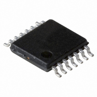
P87LPC760BDH,112 NXP Semiconductors, P87LPC760BDH,112 Datasheet - Page 34

P87LPC760BDH,112
Manufacturer Part Number
P87LPC760BDH,112
Description
IC 80C51 MCU 1K OTP 14-TSSOP
Manufacturer
NXP Semiconductors
Series
LPC700r
Datasheet
1.P87LPC760BN112.pdf
(56 pages)
Specifications of P87LPC760BDH,112
Program Memory Type
OTP
Program Memory Size
1KB (1K x 8)
Package / Case
14-TSSOP
Core Processor
8051
Core Size
8-Bit
Speed
20MHz
Connectivity
I²C, UART/USART
Peripherals
Brown-out Detect/Reset, LED, POR, WDT
Number Of I /o
12
Ram Size
128 x 8
Voltage - Supply (vcc/vdd)
2.7 V ~ 6 V
Oscillator Type
Internal
Operating Temperature
0°C ~ 70°C
Processor Series
P87LPC7x
Core
80C51
Data Bus Width
8 bit
Data Ram Size
128 B
Interface Type
I2C/UART
Maximum Clock Frequency
20 MHz
Number Of Programmable I/os
12
Number Of Timers
2
Operating Supply Voltage
2.7 V to 6 V
Maximum Operating Temperature
+ 70 C
Mounting Style
SMD/SMT
3rd Party Development Tools
PK51, CA51, A51, ULINK2
Minimum Operating Temperature
0 C
Lead Free Status / RoHS Status
Lead free / RoHS Compliant
For Use With
OM10063 - PROGRAMMER LPC700 P76XLCPOM10050 - EMULATOR LPC700 PDS76X
Eeprom Size
-
Data Converters
-
Lead Free Status / Rohs Status
Lead free / RoHS Compliant
Other names
568-1015-5
935271146112
P87LPC760BDH
935271146112
P87LPC760BDH
Philips Semiconductors
Timer Overflow Toggle Output
Timer 0 can be configured to automatically toggle a port output
whenever a timer overflow occurs. The same device pins that is
used for the T0 count inputs are also used for the timer toggle
outputs. This function is enabled by control bit T0OE in the P2M1
register. The port outputs will be a logic 1 prior to the first timer
overflow when this mode is turned on.
UART
The P87LPC760 includes an enhanced 80C51 UART. The baud rate
source for the UART is timer 1 for modes 1 and 3, while the rate is
fixed in modes 0 and 2. Because CPU clocking is different on the
P87LPC760 than on the standard 80C51, baud rate calculation is
somewhat different. Enhancements over the standard 80C51 UART
include Framing Error detection and automatic address recognition.
The serial port is full duplex, meaning it can transmit and receive
simultaneously. It is also receive-buffered, meaning it can
commence reception of a second byte before a previously received
byte has been read from the SBUF register. However, if the first byte
still hasn’t been read by the time reception of the second byte is
complete, the first byte will be lost. The serial port receive and
transmit registers are both accessed through Special Function
Register SBUF. Writing to SBUF loads the transmit register, and
reading SBUF accesses a physically separate receive register.
The serial port can be operated in 4 modes:
Mode 0
Serial data enters and exits through RxD. TxD outputs the shift
clock. 8 bits are transmitted or received, LSB first. The baud rate is
fixed at 1/6 of the CPU clock frequency.
Mode 1
10 bits are transmitted (through TxD) or received (through RxD): a
start bit (logical 0), 8 data bits (LSB first), and a stop bit (logical 1).
When data is received, the stop bit is stored in RB8 in Special
Function Register SCON. The baud rate is variable and is
determined by the Timer 1 overflow rate.
2002 Mar 07
Low power, low price, low pin count (14 pin)
microcontroller with 1 kbyte OTP
31
uses SBUF as a destination register. Reception is initiated in Mode 0
Mode 2
11 bits are transmitted (through TxD) or received (through RxD):
start bit (logical 0), 8 data bits (LSB first), a programmable 9th data
bit, and a stop bit (logical 1). When data is transmitted, the 9th data
bit (TB8 in SCON) can be assigned the value of 0 or 1. Or, for
example, the parity bit (P, in the PSW) could be moved into TB8.
When data is received, the 9th data bit goes into RB8 in Special
Function Register SCON, while the stop bit is ignored. The baud
rate is programmable to either 1/16 or 1/32 of the CPU clock
frequency, as determined by the SMOD1 bit in PCON.
Mode 3
11 bits are transmitted (through TxD) or received (through RxD): a
start bit (logical 0), 8 data bits (LSB first), a programmable 9th data
bit, and a stop bit (logical 1). In fact, Mode 3 is the same as Mode 2
in all respects except baud rate. The baud rate in Mode 3 is variable
and is determined by the Timer 1 overflow rate.
In all four modes, transmission is initiated by any instruction that
by the condition RI = 0 and REN = 1. Reception is initiated in the
other modes by the incoming start bit if REN = 1
Serial Port Control Register (SCON)
The serial port control and status register is the Special Function
Register SCON, shown in Figure 31. This register contains not only
the mode selection bits, but also the 9th data bit for transmit and
receive (TB8 and RB8), and the serial port interrupt bits (TI and RI).
The Framing Error bit (FE) allows detection of missing stop bits in
the received data stream. The FE bit shares the bit position SCON.7
with the SM0 bit. Which bit appears in SCON at any particular time
is determined by the SMOD0 bit in the PCON register. If SMOD0 =
0, SCON.7 is the SM0 bit. If SMOD0 = 1, SCON.7 is the FE bit.
Once set, the FE bit remains set until it is cleared by software. This
allows detection of framing errors for a group of characters without
the need for monitoring it for every character individually.
P87LPC760
Preliminary data


