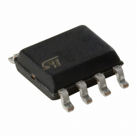
ST7FLITEU09M6 STMicroelectronics, ST7FLITEU09M6 Datasheet - Page 15

ST7FLITEU09M6
Manufacturer Part Number
ST7FLITEU09M6
Description
MCU 8BIT SGL VOLT FLASH SO-8
Manufacturer
STMicroelectronics
Series
ST7r
Datasheet
1.ST7FLITEU05M6.pdf
(139 pages)
Specifications of ST7FLITEU09M6
Core Processor
ST7
Core Size
8-Bit
Speed
8MHz
Peripherals
LVD, POR, PWM, WDT
Number Of I /o
5
Program Memory Size
2KB (2K x 8)
Program Memory Type
FLASH
Eeprom Size
128 x 8
Ram Size
128 x 8
Voltage - Supply (vcc/vdd)
2.4 V ~ 5.5 V
Data Converters
A/D 5x10b
Oscillator Type
Internal
Operating Temperature
-40°C ~ 85°C
Package / Case
8-SOIC (3.9mm Width)
Processor Series
ST7FLITEUx
Core
ST7
Data Bus Width
8 bit
Data Ram Size
128 B
Interface Type
ICC
Maximum Clock Frequency
8 MHz
Number Of Programmable I/os
5
Number Of Timers
2
Maximum Operating Temperature
+ 85 C
Mounting Style
SMD/SMT
Development Tools By Supplier
ST7FLITE-SK/RAIS, ST7FLITU0-D/RAIS, STX-RLINK
Minimum Operating Temperature
- 40 C
On-chip Adc
10 bit, 5 Channel
Cpu Family
ST7
Device Core Size
8b
Frequency (max)
8MHz
Total Internal Ram Size
128Byte
# I/os (max)
5
Number Of Timers - General Purpose
2
Operating Supply Voltage (typ)
5V
Operating Supply Voltage (max)
5.5V
Operating Supply Voltage (min)
3.3V
Instruction Set Architecture
CISC
Operating Temp Range
-40C to 85C
Operating Temperature Classification
Industrial
Mounting
Surface Mount
Pin Count
8
Package Type
SO N
For Use With
497-5858 - EVAL BOARD PLAYBACK ST7FLITE
Lead Free Status / RoHS Status
Lead free / RoHS Compliant
Connectivity
-
Lead Free Status / Rohs Status
Details
Available stocks
Company
Part Number
Manufacturer
Quantity
Price
Company:
Part Number:
ST7FLITEU09M6TR
Manufacturer:
MICROCHIP
Quantity:
12 000
ST7LITEU05 ST7LITEU09
Table 2.
1.
2. After a reset, the multiplexed PA3/RESET pin will act as RESET. To configure this pin as output (Port A3), write 55h to
1
2
3
4
5
6
7
8
MUXCR0 and AAh to MUXCR1. For further details, please refer to
It is mandatory to connect all available V
V
PA5/AIN4/CLKIN
PA4/AIN3/MCO
PA3/RESET
PA2/AIN2/LTIC
PA1/AIN1/ICCCLK
PA0/AIN0/ATPWM/
ICCDATA
V
DD
SS
(1)
(1)
Pin Name
Legend / Abbreviations for
Type: I = input, O = output, S = supply
In/Output level: C
Output level: HS = High sink (on N-buffer only)
Port and control configuration:
●
●
The RESET configuration of each pin is shown in bold which is valid as long as the device is
in reset state.
Device pin description
(2)
Input: float = floating, wpu = weak pull-up, int = interrupt, ana = analog
Output: OD = open drain, PP = push-pull
I/O C
I/O C
I/O C
I/O C
I/O C
O
S
S
T
T
T
T
T
Level
T
= CMOS 0.3 V
HS
HS
HS
HS
HS
DD
and V
X
X
X
X
X
Table
DDA
X
Input
Port / Control
ei1
ei4
ei3
ei2
ei0
DD
pins to the supply voltage and all V
2:
/0.7 V
X
X
X
X
X
DD
Output
X
X
X
X
X
X
Section 7.5 on page
with input trigger
X
X
X
X
X
X
Main power supply
Port A5
Port A4
Port A3
Port A2
Port A1
Port A0
Ground
function
reset)
(after
main
41.
Analog input 4 or external clock
input
Analog input 3 or main clock
output
RESET
Analog input 2 or lite timer input
capture
Analog input 1 or In Circuit
Communication Clock
Caution: During normal
operation this pin must be pulled-
up, internally or externally
(external pull-up of 10k
mandatory in noisy
environment). This is to avoid
entering ICC mode unexpectedly
during a reset. In the application,
even if the pin is configured as
output, any reset will put it back
in pull-up
Analog input 0 or Auto-Reload
Timer PWM or In Circuit
Communication Data
SS
and V
Alternate function
(2)
SSA
pins to ground.
Pin description
15/139


