ST7FLI49MK1T6 STMicroelectronics, ST7FLI49MK1T6 Datasheet - Page 129
ST7FLI49MK1T6
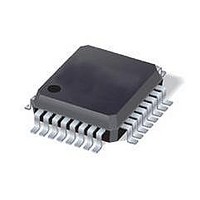
Manufacturer Part Number
ST7FLI49MK1T6
Description
MCU 8BIT SGL VOLT FLASH 32-LQFP
Manufacturer
STMicroelectronics
Series
ST7r
Datasheet
1.ST7FLI49MK1T6TR.pdf
(187 pages)
Specifications of ST7FLI49MK1T6
Core Processor
ST7
Core Size
8-Bit
Speed
8MHz
Connectivity
I²C
Peripherals
LVD, POR, PWM, WDT
Number Of I /o
24
Program Memory Size
4KB (4K x 8)
Program Memory Type
FLASH
Eeprom Size
128 x 8
Ram Size
384 x 8
Voltage - Supply (vcc/vdd)
2.4 V ~ 5.5 V
Data Converters
A/D 10x10b
Oscillator Type
Internal
Operating Temperature
-40°C ~ 85°C
Package / Case
32-LQFP
Processor Series
ST7FLI4x
Core
ST7
Data Bus Width
8 bit
Data Ram Size
384 B
Interface Type
I2C
Maximum Clock Frequency
8 MHz
Number Of Programmable I/os
24
Number Of Timers
5
Maximum Operating Temperature
+ 125 C
Mounting Style
SMD/SMT
Minimum Operating Temperature
- 40 C
On-chip Adc
10 bit, 10 Channel
Lead Free Status / RoHS Status
Lead free / RoHS Compliant
Available stocks
Company
Part Number
Manufacturer
Quantity
Price
Company:

Part Number:
ST7FLI49MK1T6
Manufacturer:
st
Quantity:
456
Company:
Part Number:
ST7FLI49MK1T6
Manufacturer:
STMicroelectronics
Quantity:
10 000
Part Number:
ST7FLI49MK1T6
Manufacturer:
ST
Quantity:
20 000
Company:
Part Number:
ST7FLI49MK1T6TR
Manufacturer:
STMicroelectronics
Quantity:
10 000


ST7LITE49M
Data register high (ADCDRH)
Reset value: xxxx xxxx (xxh)
Bits 7:0 = D[9:2] MSB of analog converted value
ADC control/data register low (ADCDRL)
Reset value: 0000 00xx (0xh)
Bits 7:4 = Reserved. Forced by hardware to 0.
Bit 3 = SLOW Slow mode bit
Table 48.
1. The maximum allowed value of f
Bit 2 = Reserved. Forced by hardware to 0.
Bits 1:0 = D[1:0] LSB of analog converted value
Table 49.
Address
(Hex.)
0036h
0037h
0038h
D9
This bit is set and cleared by software. It is used together with the SPEED bit in the
ADCCSR register to configure the ADC clock speed as shown on the table below.
7
0
7
Reset value
Reset value
Reset value
ADCDRH
ADCCSR
ADCDRL
Register
Configuring the ADC clock speed
ADC register mapping and reset values
label
D8
0
EOC
D9
7
0
x
0
0
D7
0
f
f
f
ADC
ADC
CPU
CPU
f
Doc ID 13562 Rev 3
CPU
SPEED
is 4 MHz (see
(1)
/2
/4
D8
6
0
x
0
0
D6
0
ADON
Read/write
Read only
D7
5
0
x
0
0
Section 13.11 on page
SLOW
D5
D6
4
0
0
0
x
SLOW
CH3
D5
3
0
x
0
D4
0
170)
SLOW
CH2
D4
0
0
1
On-chip peripherals
2
0
0
x
D3
D1
CH1
D3
D1
1
0
x
x
SPEED
0
1
x
D2
129/188
D0
0
0
CH0
D2
D0
0
0
x
x
Related parts for ST7FLI49MK1T6
Image
Part Number
Description
Manufacturer
Datasheet
Request
R

Part Number:
Description:
BOARD DAUGHTER 32LQFP ST7FLITE4
Manufacturer:
STMicroelectronics
Datasheet:
Part Number:
Description:
STMicroelectronics [RIPPLE-CARRY BINARY COUNTER/DIVIDERS]
Manufacturer:
STMicroelectronics
Datasheet:
Part Number:
Description:
STMicroelectronics [LIQUID-CRYSTAL DISPLAY DRIVERS]
Manufacturer:
STMicroelectronics
Datasheet:

Part Number:
Description:
BOARD EVAL FOR MEMS SENSORS
Manufacturer:
STMicroelectronics
Datasheet:
Part Number:
Description:
NPN TRANSISTOR POWER MODULE
Manufacturer:
STMicroelectronics
Datasheet:
Part Number:
Description:
TURBOSWITCH ULTRA-FAST HIGH VOLTAGE DIODE
Manufacturer:
STMicroelectronics
Datasheet:
Part Number:
Description:
Manufacturer:
STMicroelectronics
Datasheet:
Part Number:
Description:
DIODE / SCR MODULE
Manufacturer:
STMicroelectronics
Datasheet:
Part Number:
Description:
DIODE / SCR MODULE
Manufacturer:
STMicroelectronics
Datasheet:
Part Number:
Description:
Search -----> STE16N100
Manufacturer:
STMicroelectronics
Datasheet:
Part Number:
Description:
Search ---> STE53NA50
Manufacturer:
STMicroelectronics
Datasheet:
Part Number:
Description:
NPN Transistor Power Module
Manufacturer:
STMicroelectronics
Datasheet: