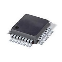
ST7FLI49MK1T6 STMicroelectronics, ST7FLI49MK1T6 Datasheet - Page 170

ST7FLI49MK1T6
Manufacturer Part Number
ST7FLI49MK1T6
Description
MCU 8BIT SGL VOLT FLASH 32-LQFP
Manufacturer
STMicroelectronics
Series
ST7r
Datasheet
1.ST7FLI49MK1T6TR.pdf
(187 pages)
Specifications of ST7FLI49MK1T6
Core Processor
ST7
Core Size
8-Bit
Speed
8MHz
Connectivity
I²C
Peripherals
LVD, POR, PWM, WDT
Number Of I /o
24
Program Memory Size
4KB (4K x 8)
Program Memory Type
FLASH
Eeprom Size
128 x 8
Ram Size
384 x 8
Voltage - Supply (vcc/vdd)
2.4 V ~ 5.5 V
Data Converters
A/D 10x10b
Oscillator Type
Internal
Operating Temperature
-40°C ~ 85°C
Package / Case
32-LQFP
Processor Series
ST7FLI4x
Core
ST7
Data Bus Width
8 bit
Data Ram Size
384 B
Interface Type
I2C
Maximum Clock Frequency
8 MHz
Number Of Programmable I/os
24
Number Of Timers
5
Maximum Operating Temperature
+ 125 C
Mounting Style
SMD/SMT
Minimum Operating Temperature
- 40 C
On-chip Adc
10 bit, 10 Channel
Lead Free Status / RoHS Status
Lead free / RoHS Compliant
Available stocks
Company
Part Number
Manufacturer
Quantity
Price
Company:
Part Number:
ST7FLI49MK1T6
Manufacturer:
st
Quantity:
456
Company:
Part Number:
ST7FLI49MK1T6
Manufacturer:
STMicroelectronics
Quantity:
10 000
Part Number:
ST7FLI49MK1T6
Manufacturer:
ST
Quantity:
20 000
Company:
Part Number:
ST7FLI49MK1T6TR
Manufacturer:
STMicroelectronics
Quantity:
10 000
Electrical characteristics
13.11
Table 86.
1. Unless otherwise specified, typical data are based on T
2. The maximum ADC clock frequency allowed within V
3. Any added external serial resistor will downgrade the ADC accuracy (especially for resistance greater than the maximum
4. The stabilization time of the A/D converter is masked by the first t
170/188
Symbol
C
t
R
f
V
t
STAB
ADC
ADC
guidelines and are not tested.
value). Data guaranteed by Design, not tested in production.
valid.
ADC
AIN
AIN
Conversion time (Sample+Hold)
- Sample capacitor loading time
Stabilization time after ADC
Figure 97. RESET pin protection when LVD is disabled
1. The reset network protects the device against parasitic resets.
2. Please refer to
10-bit ADC characteristics
Subject to general operating condition for V
ADC characteristics
Conversion voltage range
Internal sample and hold
ADC clock frequency
- Hold conversion time
External input resistor
The output of the external reset circuit must have an open-drain output to drive the ST7 reset pad.
Otherwise the device can be damaged when the ST7 generates an internal reset (LVD or watchdog).
Whatever the reset source is (internal or external), the user must ensure that the level on the RESET pin
can go below the V
taken into account internally.
Because the reset circuit is designed to allow the internal reset to be output in the RESET pin, the user
must ensure that the current sunk on the RESET pin is less than the absolute maximum value specified for
I
INJ(RESET)
Required
EXTERNAL
CIRCUIT
RESET
USER
Parameter
capacitor
enable
in
Section Table 59. on page
Section 12.2.1 on page 136
IL
0.01μF
(2)
max. level specified in
2.7 V ≤ V
2.4 V ≤ V
Doc ID 13562 Rev 3
f
V
CPU
V
DD
DD
DD
= 8 MHz, f
A
= 2.4 V to 2.7 V operating range is 1 MHz.
141.
= 3.3 V, f
= 25 °C and V
DD
DD
= 5 V, f
Conditions
for more details on illegal opcode reset conditions.
V
Section 13.10.1 on page
≤5.5 V, f
≤2.7 V, f
DD
R
LOAD
ADC
ON
DD
ADC
ADC
Filter
= 4 MHz
, f
. The first conversion after the enable is then always
= 4 MHz
= 4 MHz
ADC
ADC
DD
OSC
GENERATOR
= 2 MHz
= 1 MHz
-V
SS
, and T
PULSE
= 5 V. They are given only as design
A
168. Otherwise the reset will not be
V
unless otherwise specified.
Min
SSA
Typ
0
3.5
10
6
4
(4)
(1)
WATCHDOG
ILLEGAL OPCODE
V
INTERNAL
RESET
10
20
Max
8
7
DDA
4
(3)
(3)
ST7LITE49M
(3)
(3)
ST7XXX
1/f
MHz
Unit
kΩ
pF
μs
V
ADC


