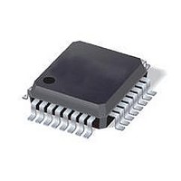
ST7FLI49MK1T6 STMicroelectronics, ST7FLI49MK1T6 Datasheet - Page 27

ST7FLI49MK1T6
Manufacturer Part Number
ST7FLI49MK1T6
Description
MCU 8BIT SGL VOLT FLASH 32-LQFP
Manufacturer
STMicroelectronics
Series
ST7r
Datasheet
1.ST7FLI49MK1T6TR.pdf
(187 pages)
Specifications of ST7FLI49MK1T6
Core Processor
ST7
Core Size
8-Bit
Speed
8MHz
Connectivity
I²C
Peripherals
LVD, POR, PWM, WDT
Number Of I /o
24
Program Memory Size
4KB (4K x 8)
Program Memory Type
FLASH
Eeprom Size
128 x 8
Ram Size
384 x 8
Voltage - Supply (vcc/vdd)
2.4 V ~ 5.5 V
Data Converters
A/D 10x10b
Oscillator Type
Internal
Operating Temperature
-40°C ~ 85°C
Package / Case
32-LQFP
Processor Series
ST7FLI4x
Core
ST7
Data Bus Width
8 bit
Data Ram Size
384 B
Interface Type
I2C
Maximum Clock Frequency
8 MHz
Number Of Programmable I/os
24
Number Of Timers
5
Maximum Operating Temperature
+ 125 C
Mounting Style
SMD/SMT
Minimum Operating Temperature
- 40 C
On-chip Adc
10 bit, 10 Channel
Lead Free Status / RoHS Status
Lead free / RoHS Compliant
Available stocks
Company
Part Number
Manufacturer
Quantity
Price
Company:
Part Number:
ST7FLI49MK1T6
Manufacturer:
st
Quantity:
456
Company:
Part Number:
ST7FLI49MK1T6
Manufacturer:
STMicroelectronics
Quantity:
10 000
Part Number:
ST7FLI49MK1T6
Manufacturer:
ST
Quantity:
20 000
Company:
Part Number:
ST7FLI49MK1T6TR
Manufacturer:
STMicroelectronics
Quantity:
10 000
ST7LITE49M
5.6
Note:
5.7
Note:
Data EEPROM read-out protection
The read-out protection is enabled through an option bit (see
When this option is selected, the programs and data stored in the EEPROM memory are
protected against Read-out (including a re-write protection). In Flash devices, when this
protection is removed by reprogramming the option byte, the entire Program memory and
EEPROM is first automatically erased.
Both program memory and data EEPROM are protected using the same option bit.
Figure 9.
EEPROM control/status register (EECSR)
Address: 0035h
Reset value: 0000 0000 (00h)
Bits 7:2 = Reserved, forced by hardware to 0
Bit 1 = E2LAT Latch access transfer bit: this bit is set by software.
Bit 0 = E2PGM Programming control and status bit
If the E2PGM bit is cleared during the programming cycle, the memory data is not
guaranteed.
Internal
Programming
voltage
0: Read mode
1: Write mode
It is cleared by hardware at the end of the programming cycle. It can only be cleared by
software if the E2PGM bit is cleared
This bit is set by software to begin the programming cycle. At the end of the
programming cycle, this bit is cleared by hardware.
0: Programming finished or not yet started
1: Programming cycle is in progress
7
0
Data EEPROM programming cycle
DATA LATCHES
WRITE OF
0
READ OPERATION NOT POSSIBLE
0
ERASE CYCLE
Doc ID 13562 Rev 3
0
t
Read/write
PROG
WRITE CYCLE
0
Section 14.1: Option
0
READ OPERATION POSSIBLE
E2LAT
LAT
PGM
Data EEPROM
E2PGM
bytes).
0
27/188


