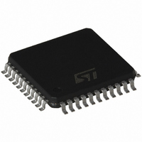
ST72F561J4T6 STMicroelectronics, ST72F561J4T6 Datasheet - Page 253

ST72F561J4T6
Manufacturer Part Number
ST72F561J4T6
Description
IC MCU 8BIT 16K FLASH 44-LQFP
Manufacturer
STMicroelectronics
Series
ST7r
Datasheet
1.ST72F561K6T6.pdf
(265 pages)
Specifications of ST72F561J4T6
Core Processor
ST7
Core Size
8-Bit
Speed
8MHz
Connectivity
CAN, LINSCI, SPI
Peripherals
LVD, POR, PWM, WDT
Number Of I /o
32
Program Memory Size
16KB (16K x 8)
Program Memory Type
FLASH
Ram Size
1K x 8
Voltage - Supply (vcc/vdd)
3.8 V ~ 5.5 V
Data Converters
A/D 16x10b
Oscillator Type
External
Operating Temperature
-40°C ~ 85°C
Package / Case
44-LQFP
Processor Series
ST72F5x
Core
ST7
Data Bus Width
8 bit
Data Ram Size
1 KB
Interface Type
CAN, SCI, SPI
Maximum Clock Frequency
8 MHz
Number Of Programmable I/os
48
Number Of Timers
3
Maximum Operating Temperature
+ 85 C
Mounting Style
SMD/SMT
Development Tools By Supplier
STX-RLINK
Minimum Operating Temperature
- 40 C
On-chip Adc
10 bit, 16 Channel
For Use With
497-8374 - BOARD DEVELOPMENT FOR ST72F561
Lead Free Status / RoHS Status
Lead free / RoHS Compliant
Eeprom Size
-
Lead Free Status / Rohs Status
Details
Available stocks
Company
Part Number
Manufacturer
Quantity
Price
Company:
Part Number:
ST72F561J4T6
Manufacturer:
COILCRAFT
Quantity:
4 000
Company:
Part Number:
ST72F561J4T6
Manufacturer:
STMicroelectronics
Quantity:
10 000
- Current page: 253 of 265
- Download datasheet (10Mb)
FLASH OPTION BYTES (Cont’d)
OPT2:1 = PKG[1:0] Package selection
These option bits select the device package.
Note: Pads that are not bonded to external pins
are in input pull-up configuration when the pack-
age selection option bits have been properly pro-
grammed. The configuration of these pads must
be kept in reset state to avoid added current con-
sumption.
OPT0 = FMP_R Flash memory read-out protec-
tion
Read-out protection, when selected provides a
protection against program memory content ex-
traction and against write access to Flash memo-
ry. Erasing the option bytes when the FMP_R op-
tion is selected causes the whole user memory to
be erased first, and the device can be repro-
grammed. Refer to
Flash Programming Reference Manual for more
details.
0: Read-out protection enabled
1: Read-out protection disabled
OPTION BYTE 1
OPT7:6 = AFI_MAP[1:0] AFI Mapping
These option bits allow the mapping of some of the
Alternate Functions to be changed.
T16_OCMP1 on PD3
T16_OCMP2 on PD5
T16_ICAP1 on PD4
LINSCI2_SCK not available
LINSCI2_TDO not available
LINSCI2_RDI not available
T16_OCMP1 on PB6
T16_OCMP2 on PB7
T16_ICAP1 on PC0
LINSCI2_SCK on PD3
LINSCI2_TDO on PD5
LINSCI2_RDI on PD4
Selected Package
AFI Mapping 1
LQFP 64
LQFP 44
LQFP 32
Section 4.3.1
and the ST7
1
1
0
0
AFI_MAP(1)
PKG
0
1
0
x
1
0
OPT5:4 = OSCTYPE[1:0] Oscillator Type
These option bits select the ST7 main clock
source type.
OPT3:2 = OSCRANGE[1:0] Oscillator range
If the resonator oscillator type is selected, these
option bits select the resonator oscillator. This se-
lection corresponds to the frequency range of the
resonator used. If external source is selected with
the OSCTYPE option, then the OSCRANGE op-
tion must be selected with the corresponding
range.
OPT1 = Reserved
OPT0 = RSTC RESET clock cycle selection
This option bit selects the number of CPU cycles
inserted during the RESET phase and when exit-
ing HALT mode. For resonator oscillators, it is ad-
vised to select 4096 due to the long crystal stabili-
zation time.
0: Reset phase with 4096 CPU cycles
1: Reset phase with 256 CPU cycles
Resonator Oscillator
Reserved
Reserved internal clock source
(used only in ICC mode)
External Source
LP
MP
MS
HS
T16_ICAP2 is mapped on PD1
T16_ICAP2 is mapped on PC1
Typ. Freq. Range
Clock Source
AFI Mapping 0
8~16 MHz
1~2 MHz
2~4 MHz
4~8 MHz
OSCRANGE
1
0
0
1
1
1
0
0
1
1
OSCTYPE
AFI_MAP(0)
ST72561
0
1
253/265
0
0
1
0
1
0
0
1
0
1
Related parts for ST72F561J4T6
Image
Part Number
Description
Manufacturer
Datasheet
Request
R

Part Number:
Description:
STMicroelectronics [RIPPLE-CARRY BINARY COUNTER/DIVIDERS]
Manufacturer:
STMicroelectronics
Datasheet:

Part Number:
Description:
STMicroelectronics [LIQUID-CRYSTAL DISPLAY DRIVERS]
Manufacturer:
STMicroelectronics
Datasheet:

Part Number:
Description:
BOARD EVAL FOR MEMS SENSORS
Manufacturer:
STMicroelectronics
Datasheet:

Part Number:
Description:
NPN TRANSISTOR POWER MODULE
Manufacturer:
STMicroelectronics
Datasheet:

Part Number:
Description:
TURBOSWITCH ULTRA-FAST HIGH VOLTAGE DIODE
Manufacturer:
STMicroelectronics
Datasheet:

Part Number:
Description:
Manufacturer:
STMicroelectronics
Datasheet:

Part Number:
Description:
DIODE / SCR MODULE
Manufacturer:
STMicroelectronics
Datasheet:

Part Number:
Description:
DIODE / SCR MODULE
Manufacturer:
STMicroelectronics
Datasheet:

Part Number:
Description:
Search -----> STE16N100
Manufacturer:
STMicroelectronics
Datasheet:

Part Number:
Description:
Search ---> STE53NA50
Manufacturer:
STMicroelectronics
Datasheet:

Part Number:
Description:
NPN Transistor Power Module
Manufacturer:
STMicroelectronics
Datasheet:

Part Number:
Description:
DIODE / SCR MODULE
Manufacturer:
STMicroelectronics
Datasheet:


