MC9S08AC16CFGE Freescale Semiconductor, MC9S08AC16CFGE Datasheet - Page 50
MC9S08AC16CFGE
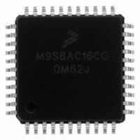
Manufacturer Part Number
MC9S08AC16CFGE
Description
IC MCU 8BIT 16K FLASH 44-LQFP
Manufacturer
Freescale Semiconductor
Series
HCS08r
Datasheet
1.MC9S08AC8CFGE.pdf
(336 pages)
Specifications of MC9S08AC16CFGE
Core Processor
HCS08
Core Size
8-Bit
Speed
40MHz
Connectivity
I²C, SCI, SPI
Peripherals
LVD, POR, PWM, WDT
Number Of I /o
34
Program Memory Size
16KB (16K x 8)
Program Memory Type
FLASH
Ram Size
1K x 8
Voltage - Supply (vcc/vdd)
2.7 V ~ 5.5 V
Data Converters
A/D 8x10b
Oscillator Type
Internal
Operating Temperature
-40°C ~ 85°C
Package / Case
44-LQFP
Package
44LQFP
Family Name
HCS08
Maximum Speed
40 MHz
Operating Supply Voltage
3.3|5 V
Data Bus Width
8 Bit
Number Of Programmable I/os
34
Interface Type
I2C/SCI/SPI
On-chip Adc
8-chx10-bit
Number Of Timers
8
Processor Series
S08AC
Core
HCS08
Data Ram Size
1 KB
Maximum Clock Frequency
40 MHz
Maximum Operating Temperature
+ 85 C
Mounting Style
SMD/SMT
3rd Party Development Tools
EWS08
Development Tools By Supplier
DEMO9S08AC60E, DEMOACEX, DEMOACKIT, DCF51AC256, DC9S08AC128, DC9S08AC16, DC9S08AC60, DEMO51AC256KIT
Minimum Operating Temperature
- 40 C
Cpu Family
HCS08
Device Core Size
8b
Frequency (max)
40MHz
Total Internal Ram Size
1KB
# I/os (max)
34
Number Of Timers - General Purpose
8
Operating Supply Voltage (typ)
3.3/5V
Operating Supply Voltage (max)
5.5V
Operating Supply Voltage (min)
2.7V
Instruction Set Architecture
CISC
Operating Temp Range
-40C to 85C
Operating Temperature Classification
Industrial
Mounting
Surface Mount
Pin Count
44
Package Type
LQFP
Lead Free Status / RoHS Status
Lead free / RoHS Compliant
Eeprom Size
-
Lead Free Status / Rohs Status
Lead free / RoHS Compliant
Available stocks
Company
Part Number
Manufacturer
Quantity
Price
Company:

Part Number:
MC9S08AC16CFGE
Manufacturer:
FREESCAL
Quantity:
4 000
Company:
Part Number:
MC9S08AC16CFGE
Manufacturer:
Freescale Semiconductor
Quantity:
10 000
Part Number:
MC9S08AC16CFGE
Manufacturer:
FREESCALE
Quantity:
20 000
Company:
Part Number:
MC9S08AC16CFGER
Manufacturer:
Freescale Semiconductor
Quantity:
10 000


Chapter 4 Memory
When security is enabled, the RAM is considered a secure memory resource and is not accessible through
BDM or through code executing from non-secure memory. See
description of the security feature.
4.4
The FLASH memory is intended primarily for program storage. In-circuit programming allows the
operating program to be loaded into the FLASH memory after final assembly of the application product.
It is possible to program the entire array through the single-wire background debug interface. Because no
special voltages are needed for FLASH erase and programming operations, in-application programming
is also possible through other software-controlled communication paths. For a more detailed discussion of
in-circuit and in-application programming, refer to the HCS08 Family Reference Manual, Volume I,
Freescale Semiconductor document order number HCS08RMv1/D.
4.4.1
Features of the FLASH memory include:
4.4.2
Before any program or erase command can be accepted, the FLASH clock divider register (FCDIV) must
be written to set the internal clock for the FLASH module to a frequency (f
200 kHz (see
once, so normally this write is done during reset initialization. FCDIV cannot be written if the access error
flag, FACCERR in FSTAT, is set. The user must ensure that FACCERR is not set before writing to the
FCDIV register. One period of the resulting clock (1/f
program and erase pulses. An integer number of these timing pulses are used by the command processor
to complete a program or erase command.
Table 4-5
of FCLK (f
of cycles of FCLK and as an absolute time for the case where t
shown include overhead for the command state machine and enabling and disabling of program and erase
voltages.
50
•
•
•
•
•
•
•
FLASH Size
— MC9S08AC16 and MC9S08AW16A— 16,384 bytes (32 pages of 512 bytes each)
— MC9S08AC8 and MC9S08AW8A— 8192 bytes (16 pages of 512 bytes each)
Single power supply program and erase
Command interface for fast program and erase operation
Up to 100,000 program/erase cycles at typical voltage and temperature
Flexible block protection
Security feature for FLASH and RAM
Auto power-down for low-frequency read accesses
FLASH
shows program and erase times. The bus clock frequency and FCDIV determine the frequency
Features
Program and Erase Times
FCLK
Section 4.6.1, “FLASH Clock Divider Register
). The time for one cycle of FCLK is t
MC9S08AC16 Series Data Sheet, Rev. 8
FCLK
FCLK
) is used by the command processor to time
= 1/f
(FCDIV)”). This register can be written only
FCLK
Section 4.5,
FCLK
= 5 μs. Program and erase times
. The times are shown as a number
FCLK
“Security” for a detailed
) between 150 kHz and
Freescale Semiconductor
Related parts for MC9S08AC16CFGE
Image
Part Number
Description
Manufacturer
Datasheet
Request
R

Part Number:
Description:
Manufacturer:
Freescale Semiconductor, Inc
Datasheet:
Part Number:
Description:
Manufacturer:
Freescale Semiconductor, Inc
Datasheet:
Part Number:
Description:
Manufacturer:
Freescale Semiconductor, Inc
Datasheet:
Part Number:
Description:
Manufacturer:
Freescale Semiconductor, Inc
Datasheet:
Part Number:
Description:
Manufacturer:
Freescale Semiconductor, Inc
Datasheet:
Part Number:
Description:
Manufacturer:
Freescale Semiconductor, Inc
Datasheet:
Part Number:
Description:
Manufacturer:
Freescale Semiconductor, Inc
Datasheet:
Part Number:
Description:
Manufacturer:
Freescale Semiconductor, Inc
Datasheet:
Part Number:
Description:
Manufacturer:
Freescale Semiconductor, Inc
Datasheet:
Part Number:
Description:
Manufacturer:
Freescale Semiconductor, Inc
Datasheet:
Part Number:
Description:
Manufacturer:
Freescale Semiconductor, Inc
Datasheet:
Part Number:
Description:
Manufacturer:
Freescale Semiconductor, Inc
Datasheet:
Part Number:
Description:
Manufacturer:
Freescale Semiconductor, Inc
Datasheet:
Part Number:
Description:
Manufacturer:
Freescale Semiconductor, Inc
Datasheet:
Part Number:
Description:
Manufacturer:
Freescale Semiconductor, Inc
Datasheet: