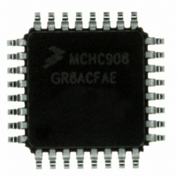
MCHC908GR8ACFAE Freescale Semiconductor, MCHC908GR8ACFAE Datasheet - Page 257

MCHC908GR8ACFAE
Manufacturer Part Number
MCHC908GR8ACFAE
Description
IC MCU 8K FLASH 8MHZ 32-LQFP
Manufacturer
Freescale Semiconductor
Series
HC08r
Specifications of MCHC908GR8ACFAE
Core Processor
HC08
Core Size
8-Bit
Speed
8MHz
Connectivity
SCI, SPI
Peripherals
LVD, POR, PWM
Number Of I /o
21
Program Memory Size
7.5KB (7.5K x 8)
Program Memory Type
FLASH
Ram Size
384 x 8
Voltage - Supply (vcc/vdd)
2.7 V ~ 5.5 V
Data Converters
A/D 6x8b
Oscillator Type
Internal
Operating Temperature
-40°C ~ 85°C
Package / Case
32-LQFP
Controller Family/series
HC08
No. Of I/o's
21
Ram Memory Size
384Byte
Cpu Speed
8MHz
No. Of Timers
2
Embedded Interface Type
I2C, SCI, SPI
Rohs Compliant
Yes
Processor Series
HC08G
Core
HC08
Data Bus Width
8 bit
Data Ram Size
384 B
Interface Type
SCI, SPI
Maximum Clock Frequency
8.2 MHz
Number Of Programmable I/os
21
Number Of Timers
3
Maximum Operating Temperature
+ 85 C
Mounting Style
SMD/SMT
Development Tools By Supplier
FSICEBASE, DEMO908GZ60E, M68CBL05CE, M68EML08GPGTE
Minimum Operating Temperature
- 40 C
On-chip Adc
8 bit, 6 Channel
Lead Free Status / RoHS Status
Lead free / RoHS Compliant
Eeprom Size
-
Lead Free Status / Rohs Status
Details
Available stocks
Company
Part Number
Manufacturer
Quantity
Price
Company:
Part Number:
MCHC908GR8ACFAE
Manufacturer:
Freescale Semiconductor
Quantity:
10 000
- Current page: 257 of 292
- Download datasheet (4Mb)
20.5 5.0-V DC Electrical Characteristics
Freescale Semiconductor
Output high voltage
Output low voltage
Input high voltage
Input low voltage
DC injection current, all ports
Total DC current injection (sum of all I/O)
I/O ports Hi-Z leakage current
Input current
Pullup resistors (as input only)
Capacitance
Monitor mode entry voltage
Low-voltage inhibit, trip falling voltage
Low-voltage inhibit, trip rising voltage
Low-voltage inhibit reset/recover hysteresis
POR rearm voltage
POR reset voltage
POR rise time ramp rate
1. V
2. Typical values reflect average measurements at midpoint of voltage range, 25°C only.
3. Some disturbance of the ADC accuracy is possible during any injection event and is dependent on board layout and power
4. Pullups and pulldowns are disabled. Port B leakage is specified in
5. Maximum is highest voltage that POR is guaranteed.
6. Maximum is highest voltage that POR is possible.
7. If minimum V
(I
(I
(I
Maximum combined I
Maximum combined I
Maximum total I
(I
(I
(I
Maximum combined I
Maximum combined I
Maximum total I
All ports, IRQ, RST, OSC1
All ports, IRQ, RST, OSC1
Ports PTA7/KBD7–PTA0/KBD0, PTC6–PTC0,
Ports (as input or output)
(V
supply decoupling. This parameter is guaranteed by characterization.
V
Load
Load
Load
Load
Load
Load
port PTD0–PTD3
port A, port B
port PTD0–PTD3
port A, port B
PTD7/T2CH1–PTD0/SS
TRIPF
DD
DD
= 5.0 Vdc ± 10%, V
is reached.
= –2.0 mA) all I/O pins
= –10.0 mA) all I/O pins
= –20.0 mA) pins PTC0–PTC4 only
= 1.6 mA) all I/O pins
= 10 mA) all I/O pins
= 20mA) pins PTC0–PTC4 only
+ V
HYS
DD
= V
OH
OL
(6)
is not reached before the internal POR reset is released, RST must be driven low externally until minimum
(5)
Characteristic
for all port pins
for all port pins
TRIPR
MC68HC908GT16 • MC68HC908GT8 • MC68HC08GT16 Data Sheet, Rev. 5.0
OH
OH
OL
OL
(7)
for port C, port E,
for port PTD4–PTD7,
)
for port C, port E,
for port PTD4–PTD7,
SS
(3)
(4)
= 0 Vdc, T
(1)
A
(3)
= T
A
(min) to T
A
(max), unless otherwise noted
V
Symbol
I
V
V
PORRST
INJTOT
R
V
V
V
I
I
I
C
V
V
V
I
I
R
V
V
V
I
TRIPR
TRIPF
OHT
V
C
OH1
OH2
V
I
OL1
OL2
OLT
POR
POR
INJ
I
I
HYS
TST
OH
OH
OH
Out
OL
OL
OL
IL
In
PU
IH
IL
In
20.16 ADC
V
V
V
V
0.7 × V
DD
DD
DD
DD
0.035
– 2.0
– 25
3.90
4.20
V
Min
20
—
—
—
—
—
—
—
—
—
—
—
—
—
—
0
0
SS
+ 2.5
Characteristics.
– 0.8
– 1.5
– 1.5
DD
5.0-V DC Electrical Characteristics
Typ
4.25
4.35
100
700
45
—
—
—
—
—
—
—
—
—
—
—
—
—
—
—
—
—
—
—
—
—
—
—
(2)
0.2 × V
V
DD
+ 2.0
Max
4.50
4.60
V
100
100
+25
±10
100
800
0.4
1.5
1.5
50
50
50
50
±1
65
12
—
—
—
—
—
8
DD
+ 4.0
DD
V/ms
Unit
mA
mA
mA
mA
mA
mA
mA
mA
mV
mV
mV
μA
μA
kΩ
pF
V
V
V
V
V
V
V
V
V
V
V
257
Related parts for MCHC908GR8ACFAE
Image
Part Number
Description
Manufacturer
Datasheet
Request
R
Part Number:
Description:
Manufacturer:
Freescale Semiconductor, Inc
Datasheet:
Part Number:
Description:
Manufacturer:
Freescale Semiconductor, Inc
Datasheet:
Part Number:
Description:
Manufacturer:
Freescale Semiconductor, Inc
Datasheet:
Part Number:
Description:
Manufacturer:
Freescale Semiconductor, Inc
Datasheet:
Part Number:
Description:
Manufacturer:
Freescale Semiconductor, Inc
Datasheet:
Part Number:
Description:
Manufacturer:
Freescale Semiconductor, Inc
Datasheet:
Part Number:
Description:
Manufacturer:
Freescale Semiconductor, Inc
Datasheet:
Part Number:
Description:
Manufacturer:
Freescale Semiconductor, Inc
Datasheet:
Part Number:
Description:
Manufacturer:
Freescale Semiconductor, Inc
Datasheet:
Part Number:
Description:
Manufacturer:
Freescale Semiconductor, Inc
Datasheet:
Part Number:
Description:
Manufacturer:
Freescale Semiconductor, Inc
Datasheet:
Part Number:
Description:
Manufacturer:
Freescale Semiconductor, Inc
Datasheet:
Part Number:
Description:
Manufacturer:
Freescale Semiconductor, Inc
Datasheet:
Part Number:
Description:
Manufacturer:
Freescale Semiconductor, Inc
Datasheet:
Part Number:
Description:
Manufacturer:
Freescale Semiconductor, Inc
Datasheet:


