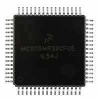
MC908MR32CFUE Freescale Semiconductor, MC908MR32CFUE Datasheet - Page 248

MC908MR32CFUE
Manufacturer Part Number
MC908MR32CFUE
Description
IC MCU 8MHZ 32K FLASH 64-QFP
Manufacturer
Freescale Semiconductor
Series
HC08r
Datasheet
1.MC908MR16CFUE.pdf
(282 pages)
Specifications of MC908MR32CFUE
Core Processor
HC08
Core Size
8-Bit
Speed
8MHz
Connectivity
SCI, SPI
Peripherals
LVD, POR, PWM
Number Of I /o
44
Program Memory Size
32KB (32K x 8)
Program Memory Type
FLASH
Ram Size
768 x 8
Voltage - Supply (vcc/vdd)
4.5 V ~ 5.5 V
Data Converters
A/D 10x10b
Oscillator Type
Internal
Operating Temperature
-40°C ~ 85°C
Package / Case
64-QFP
Processor Series
HC08MR
Core
HC08
Data Bus Width
8 bit
Data Ram Size
768 B
Interface Type
SCI/SPI
Maximum Clock Frequency
8.2 MHz
Number Of Programmable I/os
44
Number Of Timers
6
Operating Supply Voltage
0 V to 5 V
Maximum Operating Temperature
+ 85 C
Mounting Style
SMD/SMT
Development Tools By Supplier
FSICEBASE, M68CBL05CE
Minimum Operating Temperature
- 40 C
On-chip Adc
10-ch x 10-bit
Lead Free Status / RoHS Status
Lead free / RoHS Compliant
Eeprom Size
-
Lead Free Status / Rohs Status
Lead free / RoHS Compliant
Available stocks
Company
Part Number
Manufacturer
Quantity
Price
Company:
Part Number:
MC908MR32CFUE
Manufacturer:
Freescale Semiconductor
Quantity:
10 000
Part Number:
MC908MR32CFUE
Manufacturer:
NXP/恩智浦
Quantity:
20 000
- Current page: 248 of 282
- Download datasheet (2Mb)
Timer Interface B (TIMB)
MSxB — Mode Select Bit B
MSxA — Mode Select Bit A
ELSxB and ELSxA — Edge/Level Select Bits
TOVx — Toggle-On-Overflow Bit
248
This read/write bit selects buffered output compare/PWM operation. MSxB exists only in the TIMB
channel 0.
Setting MS0B disables the channel 1 status and control register and reverts TCH1B to
general-purpose I/O.
Reset clears the MSxB bit.
When ELSxB:A ≠ 00, this read/write bit selects either input capture operation or unbuffered output
compare/PWM operation. See
When ELSxB:A = 00, this read/write bit selects the initial output level of the TCHx pin once PWM, input
capture, or output compare operation is enabled. See
When channel x is an input capture channel, these read/write bits control the active edge-sensing logic
on channel x.
When channel x is an output compare channel, ELSxB and ELSxA control the channel x output
behavior when an output compare occurs.
When ELSxB and ELSxA are both clear, channel x is not connected to port E, and pin PTEx/TCHxB
is available as a general-purpose I/O pin. However, channel x is at a state determined by these bits
and becomes transparent to the respective pin when PWM, input capture, or output compare mode is
enabled.
When channel x is an output compare channel, this read/write bit controls the behavior of the channel
x output when the TIMB counter overflows. When channel x is an input capture channel, TOVx has no
effect. Reset clears the TOVx bit.
1 = Buffered output compare/PWM operation enabled
0 = Buffered output compare/PWM operation disabled
1 = Unbuffered output compare/PWM operation
0 = Input capture operation
1 = Initial output level low
0 = Initial output level high
1 = Channel x pin toggles on TIMB counter overflow.
0 = Channel x pin does not toggle on TIMB counter overflow.
Table 17-2
Before changing a channel function by writing to the MSxB or MSxA bit, set
the TSTOP and TRST bits in the TIMB status and control register (TBSC).
Before enabling a TIMB channel register for input capture operation, make
sure that the PTEx/TBCHx pin is stable for at least two bus clocks.
shows how ELSxB and ELSxA work. Reset clears the ELSxB and ELSxA bits.
MC68HC908MR32 • MC68HC908MR16 Data Sheet, Rev. 6.1
Table
17-2.
NOTE
NOTE
Table
17-2. Reset clears the MSxA bit.
Freescale Semiconductor
Related parts for MC908MR32CFUE
Image
Part Number
Description
Manufacturer
Datasheet
Request
R
Part Number:
Description:
Manufacturer:
Freescale Semiconductor, Inc
Datasheet:
Part Number:
Description:
Manufacturer:
Freescale Semiconductor, Inc
Datasheet:
Part Number:
Description:
Manufacturer:
Freescale Semiconductor, Inc
Datasheet:
Part Number:
Description:
Manufacturer:
Freescale Semiconductor, Inc
Datasheet:
Part Number:
Description:
Manufacturer:
Freescale Semiconductor, Inc
Datasheet:
Part Number:
Description:
Manufacturer:
Freescale Semiconductor, Inc
Datasheet:
Part Number:
Description:
Manufacturer:
Freescale Semiconductor, Inc
Datasheet:
Part Number:
Description:
Manufacturer:
Freescale Semiconductor, Inc
Datasheet:
Part Number:
Description:
Manufacturer:
Freescale Semiconductor, Inc
Datasheet:
Part Number:
Description:
Manufacturer:
Freescale Semiconductor, Inc
Datasheet:
Part Number:
Description:
Manufacturer:
Freescale Semiconductor, Inc
Datasheet:
Part Number:
Description:
Manufacturer:
Freescale Semiconductor, Inc
Datasheet:
Part Number:
Description:
Manufacturer:
Freescale Semiconductor, Inc
Datasheet:
Part Number:
Description:
Manufacturer:
Freescale Semiconductor, Inc
Datasheet:
Part Number:
Description:
Manufacturer:
Freescale Semiconductor, Inc
Datasheet:


