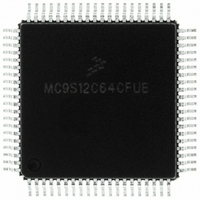
MC9S12C64CFUE Freescale Semiconductor, MC9S12C64CFUE Datasheet - Page 76

MC9S12C64CFUE
Manufacturer Part Number
MC9S12C64CFUE
Description
IC MCU 64K FLASH 4K RAM 80-QFP
Manufacturer
Freescale Semiconductor
Series
HCS12r
Specifications of MC9S12C64CFUE
Core Processor
HCS12
Core Size
16-Bit
Speed
25MHz
Connectivity
CAN, EBI/EMI, SCI, SPI
Peripherals
POR, PWM, WDT
Number Of I /o
60
Program Memory Size
64KB (64K x 8)
Program Memory Type
FLASH
Ram Size
4K x 8
Voltage - Supply (vcc/vdd)
2.35 V ~ 5.5 V
Data Converters
A/D 8x10b
Oscillator Type
Internal
Operating Temperature
-40°C ~ 85°C
Package / Case
80-QFP
Processor Series
S12C
Core
HCS12
Data Bus Width
16 bit
Data Ram Size
4 KB
Interface Type
CAN/SCI/SPI
Maximum Clock Frequency
25 MHz
Number Of Programmable I/os
60
Number Of Timers
8
Maximum Operating Temperature
+ 85 C
Mounting Style
SMD/SMT
3rd Party Development Tools
EWHCS12
Development Tools By Supplier
M68EVB912C32EE
Minimum Operating Temperature
- 40 C
On-chip Adc
8-ch x 10-bit
Package
80PQFP
Family Name
HCS12
Maximum Speed
25 MHz
Operating Supply Voltage
2.5|5 V
Height
2.4 mm
Length
14 mm
Supply Voltage (max)
2.75 V, 5.5 V
Supply Voltage (min)
2.35 V, 2.97 V
Width
14 mm
Lead Free Status / RoHS Status
Lead free / RoHS Compliant
Eeprom Size
-
Lead Free Status / Rohs Status
Lead free / RoHS Compliant
Available stocks
Company
Part Number
Manufacturer
Quantity
Price
Company:
Part Number:
MC9S12C64CFUE
Manufacturer:
Freescale Semiconductor
Quantity:
10 000
- Current page: 76 of 690
- Download datasheet (4Mb)
Chapter 2 Port Integration Module (PIM9C32) Block Description
2.2
This section lists and describes the signals that do connect off-chip.
Table 2-1
one function associated to a pin, the priority is indicated by the position in the table from top (highest
priority) to down (lowest priority).
76
Port AD
Port M
Port S
Port P
Port A
Port B
Port T
Port J
Port
Signal Description
Pin Name
shows all pins and their functions that are controlled by the PIM module. If there is more than
PAD[7:0]
PT[7:0]
PP[7:0]
PB[7:0]
PJ[7:6]
PA[7:0]
PP[6]
PM5
PM4
PM3
PM2
PM1
PM0
PS3
PS2
PS1
PS0
Pin Function
ADDR[15:8]/
DATA[15:8]/
ADDR[7:0]/
DATA[7:0]/
PWM[4:0]
PWM[5:0]
GPIO[7:0]
GPIO[7:0]
ROMON
ATD[7:0]
IOC[7:0]
RXCAN
TXCAN
GPIO
GPIO
GPIO
GPIO
GPIO
MOSI
MISO
GPIO
GPIO
GPIO
RXD
TXD
SCK
SS
Table 2-1. Pin Functions and Priorities
MC9S12C-Family / MC9S12GC-Family
PWM outputs (only available if enabled in MODRR register)
Standard timer channels
General-purpose I/O
General-purpose I/O
General purpose I/O
Serial communication interface transmit pin
General-purpose I/O
Serial communication interface receive pin
General-purpose I/O
SPI clock
SPI transmit pin
SPI slave select line
SPI receive pin
MSCAN transmit pin
MSCAN receive pin
PWM outputs
General purpose I/O with interrupt
ROMON input signal
General purpose I/O with interrupt
ATD analog inputs
General purpose I/O
Refer to MEBI Block Guide.
Refer to MEBI Block Guide.
Rev 01.24
Description
Freescale Semiconductor
Pin Function
after Reset
GPIO
Related parts for MC9S12C64CFUE
Image
Part Number
Description
Manufacturer
Datasheet
Request
R
Part Number:
Description:
Manufacturer:
Freescale Semiconductor, Inc
Datasheet:
Part Number:
Description:
Manufacturer:
Freescale Semiconductor, Inc
Datasheet:
Part Number:
Description:
Manufacturer:
Freescale Semiconductor, Inc
Datasheet:
Part Number:
Description:
Manufacturer:
Freescale Semiconductor, Inc
Datasheet:
Part Number:
Description:
Manufacturer:
Freescale Semiconductor, Inc
Datasheet:
Part Number:
Description:
Manufacturer:
Freescale Semiconductor, Inc
Datasheet:
Part Number:
Description:
Manufacturer:
Freescale Semiconductor, Inc
Datasheet:
Part Number:
Description:
Manufacturer:
Freescale Semiconductor, Inc
Datasheet:
Part Number:
Description:
Manufacturer:
Freescale Semiconductor, Inc
Datasheet:
Part Number:
Description:
Manufacturer:
Freescale Semiconductor, Inc
Datasheet:
Part Number:
Description:
Manufacturer:
Freescale Semiconductor, Inc
Datasheet:
Part Number:
Description:
Manufacturer:
Freescale Semiconductor, Inc
Datasheet:
Part Number:
Description:
Manufacturer:
Freescale Semiconductor, Inc
Datasheet:
Part Number:
Description:
Manufacturer:
Freescale Semiconductor, Inc
Datasheet:
Part Number:
Description:
Manufacturer:
Freescale Semiconductor, Inc
Datasheet:


