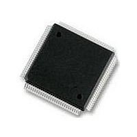
MC9S12DT256MPVE Freescale Semiconductor, MC9S12DT256MPVE Datasheet - Page 115

MC9S12DT256MPVE
Manufacturer Part Number
MC9S12DT256MPVE
Description
IC MCU 256K FLASH 25MHZ 112-LQFP
Manufacturer
Freescale Semiconductor
Series
HCS12r
Datasheet
1.S912XDG128F2MAL.pdf
(1348 pages)
Specifications of MC9S12DT256MPVE
Core Processor
HCS12
Core Size
16-Bit
Speed
25MHz
Connectivity
CAN, I²C, SCI, SPI
Peripherals
PWM, WDT
Number Of I /o
91
Program Memory Size
256KB (256K x 8)
Program Memory Type
FLASH
Eeprom Size
4K x 8
Ram Size
12K x 8
Voltage - Supply (vcc/vdd)
2.35 V ~ 5.25 V
Data Converters
A/D 8x10b
Oscillator Type
Internal
Operating Temperature
-40°C ~ 125°C
Package / Case
112-LQFP
Processor Series
S12D
Core
HCS12
Data Bus Width
16 bit
Data Ram Size
12 KB
Interface Type
CAN/I2C/SCI/SPI
Maximum Clock Frequency
25 MHz
Number Of Programmable I/os
91
Number Of Timers
1
Operating Supply Voltage
5 V to 2.5 V
Maximum Operating Temperature
+ 125 C
Mounting Style
SMD/SMT
3rd Party Development Tools
EWHCS12
Development Tools By Supplier
M68KIT912DP256
Minimum Operating Temperature
- 40 C
On-chip Adc
2 (8-ch x 10-bit)
No. Of I/o's
91
Eeprom Memory Size
4KB
Ram Memory Size
12KB
Cpu Speed
25MHz
No. Of Timers
1
No. Of Pwm Channels
8
Digital Ic Case Style
LQFP
Rohs Compliant
Yes
Lead Free Status / RoHS Status
Lead free / RoHS Compliant
Available stocks
Company
Part Number
Manufacturer
Quantity
Price
Company:
Part Number:
MC9S12DT256MPVE
Manufacturer:
Freescale Semiconductor
Quantity:
10 000
- Current page: 115 of 1348
- Download datasheet (8Mb)
2.5.2
The CRG generates a clock monitor reset in case all of the following conditions are true:
The reset event asynchronously forces the configuration registers to their default settings (see
“Memory Map and Register
doesn’t change the state of the CME bit, because it has already been set). As a consequence the CRG
immediately enters self clock mode and starts its internal reset sequence. In parallel the clock quality check
starts. As soon as clock quality check indicates a valid oscillator clock the CRG switches to OSCCLK and
leaves self clock mode. Since the clock quality checker is running in parallel to the reset generator, the
CRG may leave self clock mode while still completing the internal reset sequence. When the reset
sequence is finished, the CRG checks the internally latched state of the clock monitor fail circuit. If a clock
monitor fail is indicated, processing begins by fetching the clock monitor reset vector.
2.5.3
When COP is enabled, the CRG expects sequential write of 0x_55 and 0x_AA (in this order) to the
ARMCOP register during the selected time-out period. Once this is done, the COP time-out period restarts.
If the program fails to do this the CRG will generate a reset. Also, if any value other than 0x_55 or 0x_AA
is written, the CRG immediately generates a reset. In case windowed COP operation is enabled writes
(0x_55 or 0x_AA) to the ARMCOP register must occur in the last 25% of the selected time-out period. A
premature write the CRG will immediately generate a reset.
As soon as the reset sequence is completed the reset generator checks the reset condition. If no clock
monitor failure is indicated and the latched state of the COP timeout is true, processing begins by fetching
the COP vector.
2.5.4
The on-chip voltage regulator detects when V
on reset or low voltage reset or both. As soon as a power on reset or low voltage reset is triggered the CRG
performs a quality check on the incoming clock signal. As soon as clock quality check indicates a valid
oscillator clock signal, the reset sequence starts using the oscillator clock. If after 50 check windows the
clock quality check indicated a non-valid oscillator clock, the reset sequence starts using self-clock mode.
Figure 2-26
and when the RESET pin is held low.
Freescale Semiconductor
•
•
•
Clock monitor is enabled (CME = 1)
Loss of clock is detected
Self-clock mode is disabled (SCME = 0).
Clock Monitor Reset
Computer Operating Properly Watchdog (COP) Reset
Power On Reset, Low Voltage Reset
and
Figure 2-27
Definition”). In detail the CME and the SCME are reset to logical ‘1’ (which
show the power-up sequence for cases when the RESET pin is tied to V
MC9S12XDP512 Data Sheet, Rev. 2.21
DD
to the MCU has reached a certain level and asserts power
Chapter 2 Clocks and Reset Generator (S12CRGV6)
Section 2.3,
DD
115
Related parts for MC9S12DT256MPVE
Image
Part Number
Description
Manufacturer
Datasheet
Request
R
Part Number:
Description:
Manufacturer:
Freescale Semiconductor, Inc
Datasheet:
Part Number:
Description:
Manufacturer:
Freescale Semiconductor, Inc
Datasheet:
Part Number:
Description:
Manufacturer:
Freescale Semiconductor, Inc
Datasheet:
Part Number:
Description:
Manufacturer:
Freescale Semiconductor, Inc
Datasheet:
Part Number:
Description:
Manufacturer:
Freescale Semiconductor, Inc
Datasheet:
Part Number:
Description:
Manufacturer:
Freescale Semiconductor, Inc
Datasheet:
Part Number:
Description:
Manufacturer:
Freescale Semiconductor, Inc
Datasheet:
Part Number:
Description:
Manufacturer:
Freescale Semiconductor, Inc
Datasheet:
Part Number:
Description:
Manufacturer:
Freescale Semiconductor, Inc
Datasheet:
Part Number:
Description:
Manufacturer:
Freescale Semiconductor, Inc
Datasheet:
Part Number:
Description:
Manufacturer:
Freescale Semiconductor, Inc
Datasheet:
Part Number:
Description:
Manufacturer:
Freescale Semiconductor, Inc
Datasheet:
Part Number:
Description:
Manufacturer:
Freescale Semiconductor, Inc
Datasheet:
Part Number:
Description:
Manufacturer:
Freescale Semiconductor, Inc
Datasheet:
Part Number:
Description:
Manufacturer:
Freescale Semiconductor, Inc
Datasheet:


