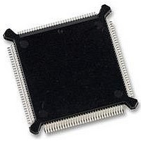
MC68331CEH20 Freescale Semiconductor, MC68331CEH20 Datasheet - Page 26

MC68331CEH20
Manufacturer Part Number
MC68331CEH20
Description
IC MCU 32BIT 20MHZ 132-PQFP
Manufacturer
Freescale Semiconductor
Series
M683xxr
Specifications of MC68331CEH20
Core Processor
CPU32
Core Size
32-Bit
Speed
20MHz
Connectivity
EBI/EMI, SCI, SPI, UART/USART
Peripherals
POR, PWM, WDT
Number Of I /o
18
Program Memory Type
ROMless
Voltage - Supply (vcc/vdd)
4.5 V ~ 5.5 V
Oscillator Type
Internal
Operating Temperature
-40°C ~ 85°C
Package / Case
132-QFP
Controller Family/series
68K
No. Of I/o's
18
Cpu Speed
20MHz
No. Of Timers
1
Embedded Interface Type
QSPI, SCI, UART
No. Of Pwm Channels
2
Digital Ic Case Style
PQFP
Rohs Compliant
Yes
Processor Series
M683xx
Core
CPU32
Data Bus Width
32 bit
Data Ram Size
80 B
Interface Type
QSPI, SCI, UART
Maximum Clock Frequency
20 MHz
Number Of Programmable I/os
18
Number Of Timers
1
Maximum Operating Temperature
+ 85 C
Mounting Style
SMD/SMT
Minimum Operating Temperature
- 40 C
Cpu Family
68K/M683xx
Device Core
ColdFire
Device Core Size
32b
Frequency (max)
20MHz
Program Memory Size
Not Required
Total Internal Ram Size
80Byte
# I/os (max)
18
Number Of Timers - General Purpose
1
Instruction Set Architecture
RISC
Operating Temp Range
-40C to 85C
Operating Temperature Classification
Industrial
Mounting
Surface Mount
Pin Count
132
Package Type
PQFP
Lead Free Status / RoHS Status
Lead free / RoHS Compliant
Eeprom Size
-
Ram Size
-
Program Memory Size
-
Data Converters
-
Lead Free Status / Rohs Status
Details
Available stocks
Company
Part Number
Manufacturer
Quantity
Price
Company:
Part Number:
MC68331CEH20
Manufacturer:
Freescale Semiconductor
Quantity:
10 000
Part Number:
MC68331CEH20
Manufacturer:
FREESCLA
Quantity:
20 000
3.4.4 Address Strobe
3.4.5 Data Bus
3.4.6 Data Strobe
3.4.7 Bus Cycle Termination Signals
3.4.8 Data Transfer Mechanism
3.4.9 Dynamic Bus Sizing
26
AS is a timing signal that indicates the validity of an address on the address bus and the validity of many
control signals. It is asserted one-half clock after the beginning of a bus cycle.
Data bus signals DATA[15:0] make up a bidirectional, non-multiplexed parallel bus that transfers data
to or from the MCU. A read or write operation can transfer 8 or 16 bits of data in one bus cycle. During
a read cycle, the data is latched by the MCU on the last falling edge of the clock for that bus cycle. For
a write cycle, all 16 bits of the data bus are driven, regardless of the port width or operand size. The
MCU places the data on the data bus one-half clock cycle after AS is asserted in a write cycle.
Data strobe (DS) is a timing signal. For a read cycle, the MCU asserts DS to signal an external device
to place data on the bus. DS is asserted at the same time as AS during a read cycle. For a write cycle,
DS signals an external device that data on the bus is valid. The MCU asserts DS one full clock cycle
after the assertion of AS during a write cycle.
During bus cycles, external devices assert the data transfer and size acknowledge signals (DSACK1
and DSACK0). During a read cycle, the signals tell the MCU to terminate the bus cycle and to latch data.
During a write cycle, the signals indicate that an external device has successfully stored data and that
the cycle can end. These signals also indicate to the MCU the size of the port for the bus cycle just com-
pleted. (Refer to 3.4.9 Dynamic Bus Sizing.)
The bus error (BERR) signal is also a bus cycle termination indicator and can be used in the absence
of DSACK1 and DSACK0 to indicate a bus error condition. It can also be asserted in conjunction with
these signals, provided it meets the appropriate timing requirements. The internal bus monitor can be
used to generate the BERR signal for internal and internal-to-external transfers. When BERR and HALT
are asserted simultaneously, the CPU takes a bus error exception.
Autovector signal (AVEC) can terminate external IRQ pin interrupt acknowledge cycles. AVEC indicates
that the MCU will internally generate a vector number to locate an interrupt handler routine. If it is con-
tinuously asserted, autovectors will be generated for all external interrupt requests. AVEC is ignored
during all other bus cycles.
The MCU architecture supports byte, word, and long-word operands, allowing access to 8- and 16-bit
data ports through the use of asynchronous cycles controlled by the data transfer and size acknowledge
inputs (DSACK1 and DSACK0).
The MCU dynamically interprets the port size of the addressed device during each bus cycle, allowing
operand transfers to or from 8- and 16-bit ports. During an operand transfer cycle, the slave device sig-
nals its port size and indicates completion of the bus cycle to the MCU through the use of the DSACK0
and DSACK1 inputs, as shown in the following table.
DSACK1
1
1
0
0
Freescale Semiconductor, Inc.
For More Information On This Product,
DSACK0
Table 10 Effect of DSACK Signals
1
0
1
0
Go to: www.freescale.com
Insert Wait States in Current Bus Cycle
Complete Cycle —Data Bus Port Size is 8 Bits
Complete Cycle —Data Bus Port Size is 16 Bits
Reserved
Result
MC68331TS/D


