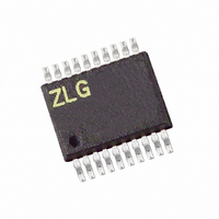
Z8F042AHH020SC00TR Zilog, Z8F042AHH020SC00TR Datasheet - Page 140

Z8F042AHH020SC00TR
Manufacturer Part Number
Z8F042AHH020SC00TR
Description
IC ENCORE XP MCU FLASH 4K 20SSOP
Manufacturer
Zilog
Series
Encore!® XP®r
Specifications of Z8F042AHH020SC00TR
Core Processor
Z8
Core Size
8-Bit
Speed
20MHz
Connectivity
IrDA, UART/USART
Peripherals
Brown-out Detect/Reset, LED, LVD, POR, PWM, Temp Sensor, WDT
Number Of I /o
17
Program Memory Size
4KB (4K x 8)
Program Memory Type
FLASH
Eeprom Size
128 x 8
Ram Size
1K x 8
Voltage - Supply (vcc/vdd)
2.7 V ~ 3.6 V
Data Converters
A/D 7x10b
Oscillator Type
Internal
Operating Temperature
0°C ~ 70°C
Package / Case
20-SSOP
Lead Free Status / RoHS Status
Contains lead / RoHS non-compliant
Other names
Z8F042AHH020SC00T
- Current page: 140 of 282
- Download datasheet (4Mb)
PS022825-0908
Input Buffer Stage
6. Add the gain correction factor to the original offset corrected value.
7. Shift the result to the right, using the sign bit determined in
Output Data
The following is the output format of the corrected ADC value.
The overflow bit in the corrected output indicates that the computed value was greater
than the maximum logical value (+1023) or less than the minimum logical value (-1024).
Unlike the hardware overflow bit, this is not a simple binary Flag. For a normal sample
(non-overflow), the sign and the overflow bit matches. If the sign bit and overflow bit do
not match, a computational overflow has occurred.
Many applications require the measurement of an input voltage source with a high output
impedance. This ADC provides a buffered input for such situations. The drawback of the
buffered input is a limitation of the input range. When using unity gain buffered mode, the
input signal must be prevented from coming too close to either V
on page 231 for details.
This condition applies only to the input voltage level (with respect to ground) of each dif-
ferential input signal. The actual differential input voltage magnitude may be less than 300
mV.
The input range of the unbuffered ADC swings from V
than 300 mV must use the unbuffered input mode. If these signals do not contain low out-
put impedances, they might require off-chip buffering.
Signals outside the allowable input range can be used without instability or device dam-
age. Any ADC readings made outside the input range are subject to greater inaccuracy
than specified.
+
=
detection of computational overflow.
s v b a 9 8 7 6
#5 MSB
#5 MSB
#1 MSB
#6 MSB
S->
MSB
#6 MSB
#5 LSB
#5 LSB
#1 LSB
#6 LSB
5 4 3 2 1 0 - -
#6 LSB
LSB
SS
Z8 Encore! XP
to V
DD
Step
SS
Product Specification
. Input signals smaller
Analog-to-Digital Converter
or V
1. This allows for the
DD
®
. See
F082A Series
Table 135
129
Related parts for Z8F042AHH020SC00TR
Image
Part Number
Description
Manufacturer
Datasheet
Request
R

Part Number:
Description:
Communication Controllers, ZILOG INTELLIGENT PERIPHERAL CONTROLLER (ZIP)
Manufacturer:
Zilog, Inc.
Datasheet:

Part Number:
Description:
KIT DEV FOR Z8 ENCORE 16K TO 64K
Manufacturer:
Zilog
Datasheet:

Part Number:
Description:
KIT DEV Z8 ENCORE XP 28-PIN
Manufacturer:
Zilog
Datasheet:

Part Number:
Description:
DEV KIT FOR Z8 ENCORE 8K/4K
Manufacturer:
Zilog
Datasheet:

Part Number:
Description:
KIT DEV Z8 ENCORE XP 28-PIN
Manufacturer:
Zilog
Datasheet:

Part Number:
Description:
DEV KIT FOR Z8 ENCORE 4K TO 8K
Manufacturer:
Zilog
Datasheet:

Part Number:
Description:
CMOS Z8 microcontroller. ROM 16 Kbytes, RAM 256 bytes, speed 16 MHz, 32 lines I/O, 3.0V to 5.5V
Manufacturer:
Zilog, Inc.
Datasheet:

Part Number:
Description:
Low-cost microcontroller. 512 bytes ROM, 61 bytes RAM, 8 MHz
Manufacturer:
Zilog, Inc.
Datasheet:

Part Number:
Description:
Z8 4K OTP Microcontroller
Manufacturer:
Zilog, Inc.
Datasheet:

Part Number:
Description:
CMOS SUPER8 ROMLESS MCU
Manufacturer:
Zilog, Inc.
Datasheet:

Part Number:
Description:
SL1866 CMOSZ8 OTP Microcontroller
Manufacturer:
Zilog, Inc.
Datasheet:

Part Number:
Description:
SL1866 CMOSZ8 OTP Microcontroller
Manufacturer:
Zilog, Inc.
Datasheet:

Part Number:
Description:
OTP (KB) = 1, RAM = 125, Speed = 12, I/O = 14, 8-bit Timers = 2, Comm Interfaces Other Features = Por, LV Protect, Voltage = 4.5-5.5V
Manufacturer:
Zilog, Inc.
Datasheet:

Part Number:
Description:
Manufacturer:
Zilog, Inc.
Datasheet:


