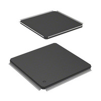
HD6417709SF133B Renesas Electronics America, HD6417709SF133B Datasheet - Page 503

HD6417709SF133B
Manufacturer Part Number
HD6417709SF133B
Description
IC SUPERH MPU ROMLESS 208LQFP
Manufacturer
Renesas Electronics America
Series
SuperH® SH7700r
Datasheet
1.D6417709SBP167BV.pdf
(809 pages)
Specifications of HD6417709SF133B
Core Processor
SH-3
Core Size
32-Bit
Speed
133MHz
Connectivity
EBI/EMI, FIFO, IrDA, SCI, SmartCard
Peripherals
DMA, POR, WDT
Number Of I /o
96
Program Memory Type
ROMless
Ram Size
16K x 8
Voltage - Supply (vcc/vdd)
1.65 V ~ 2.05 V
Data Converters
A/D 8x10b; D/A 2x8b
Oscillator Type
Internal
Operating Temperature
-20°C ~ 75°C
Package / Case
208-LQFP
Lead Free Status / RoHS Status
Contains lead / RoHS non-compliant
Eeprom Size
-
Program Memory Size
-
Available stocks
Company
Part Number
Manufacturer
Quantity
Price
Company:
Part Number:
HD6417709SF133B
Manufacturer:
RENESAS
Quantity:
79
Company:
Part Number:
HD6417709SF133B
Manufacturer:
Renesas Electronics America
Quantity:
10 000
Part Number:
HD6417709SF133B
Manufacturer:
RENESAS/瑞萨
Quantity:
20 000
Part Number:
HD6417709SF133B-V
Manufacturer:
RENESAS/瑞萨
Quantity:
20 000
Part Number:
HD6417709SF133BV
Manufacturer:
RENESAS/瑞萨
Quantity:
20 000
- Current page: 503 of 809
- Download datasheet (5Mb)
When the SCI operates on an internal clock, it can output a clock signal at the SCK pin. The
frequency of this output clock is equal to the bit rate. The phase is aligned as in figure 14.6 so that
the rising edge of the clock occurs at the center of each transmit data bit.
Transmitting and Receiving Data (SCI Initialization (Asynchronous Mode)): Before
transmitting or receiving, clear the TE and RE bits to 0 in the serial control register (SCSCR), then
initialize the SCI as follows.
When changing the operation mode or communication format, always clear the TE and RE bits to
0 before following the procedure given below. Clearing TE to 0 sets TDRE to 1 and initializes the
transmit shift register (SCTSR). Clearing RE to 0, however, does not initialize the RDRF, PER,
FER, and ORER flags or receive data register (SCRDR), which retain their previous contents.
When an external clock is used, the clock should not be stopped during initialization or subsequent
operation. SCI operation becomes unreliable if the clock is stopped.
Figure 14.7 shows a sample flowchart for initializing the SCI. The procedure for initializing the
SCI is:
1. Select the clock source in the serial control register (SCSCR). Leave RIE, TIE, TEIE, MPIE,
2. Select the communication format in the serial mode register (SCSMR).
3. Write the value corresponding to the bit rate in the bit rate register (SCBRR) (not necessary if
4. Wait for at least the interval required to transmit or receive one bit, then set TE or RE in the
TE, and RE cleared to 0. If clock output is selected in asynchronous mode, clock output starts
immediately after the setting is made in SCSCR.
an external clock is used).
serial control register (SCSCR) to 1. Also set RIE, TIE, TEIE, and MPIE as necessary. Setting
TE or RE enables the SCI to use the TxD or RxD pin. The initial state is the mark state when
transmitting, or the idle state (waiting for a start bit) when receiving.
Figure 14.6 Output Clock and Serial Data Timing (Asynchronous Mode)
0
D0
D1
D2
D3
1 frame
D4
D5
D6
D7
0/1
Rev. 5.00, 09/03, page 457 of 760
1
1
Related parts for HD6417709SF133B
Image
Part Number
Description
Manufacturer
Datasheet
Request
R

Part Number:
Description:
KIT STARTER FOR M16C/29
Manufacturer:
Renesas Electronics America
Datasheet:

Part Number:
Description:
KIT STARTER FOR R8C/2D
Manufacturer:
Renesas Electronics America
Datasheet:

Part Number:
Description:
R0K33062P STARTER KIT
Manufacturer:
Renesas Electronics America
Datasheet:

Part Number:
Description:
KIT STARTER FOR R8C/23 E8A
Manufacturer:
Renesas Electronics America
Datasheet:

Part Number:
Description:
KIT STARTER FOR R8C/25
Manufacturer:
Renesas Electronics America
Datasheet:

Part Number:
Description:
KIT STARTER H8S2456 SHARPE DSPLY
Manufacturer:
Renesas Electronics America
Datasheet:

Part Number:
Description:
KIT STARTER FOR R8C38C
Manufacturer:
Renesas Electronics America
Datasheet:

Part Number:
Description:
KIT STARTER FOR R8C35C
Manufacturer:
Renesas Electronics America
Datasheet:

Part Number:
Description:
KIT STARTER FOR R8CL3AC+LCD APPS
Manufacturer:
Renesas Electronics America
Datasheet:

Part Number:
Description:
KIT STARTER FOR RX610
Manufacturer:
Renesas Electronics America
Datasheet:

Part Number:
Description:
KIT STARTER FOR R32C/118
Manufacturer:
Renesas Electronics America
Datasheet:

Part Number:
Description:
KIT DEV RSK-R8C/26-29
Manufacturer:
Renesas Electronics America
Datasheet:

Part Number:
Description:
KIT STARTER FOR SH7124
Manufacturer:
Renesas Electronics America
Datasheet:

Part Number:
Description:
KIT STARTER FOR H8SX/1622
Manufacturer:
Renesas Electronics America
Datasheet:

Part Number:
Description:
KIT DEV FOR SH7203
Manufacturer:
Renesas Electronics America
Datasheet:


