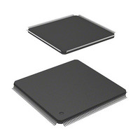
HD6417709SF133B Renesas Electronics America, HD6417709SF133B Datasheet - Page 543

HD6417709SF133B
Manufacturer Part Number
HD6417709SF133B
Description
IC SUPERH MPU ROMLESS 208LQFP
Manufacturer
Renesas Electronics America
Series
SuperH® SH7700r
Datasheet
1.D6417709SBP167BV.pdf
(809 pages)
Specifications of HD6417709SF133B
Core Processor
SH-3
Core Size
32-Bit
Speed
133MHz
Connectivity
EBI/EMI, FIFO, IrDA, SCI, SmartCard
Peripherals
DMA, POR, WDT
Number Of I /o
96
Program Memory Type
ROMless
Ram Size
16K x 8
Voltage - Supply (vcc/vdd)
1.65 V ~ 2.05 V
Data Converters
A/D 8x10b; D/A 2x8b
Oscillator Type
Internal
Operating Temperature
-20°C ~ 75°C
Package / Case
208-LQFP
Lead Free Status / RoHS Status
Contains lead / RoHS non-compliant
Eeprom Size
-
Program Memory Size
-
Available stocks
Company
Part Number
Manufacturer
Quantity
Price
Company:
Part Number:
HD6417709SF133B
Manufacturer:
RENESAS
Quantity:
79
Company:
Part Number:
HD6417709SF133B
Manufacturer:
Renesas Electronics America
Quantity:
10 000
Part Number:
HD6417709SF133B
Manufacturer:
RENESAS/瑞萨
Quantity:
20 000
Part Number:
HD6417709SF133B-V
Manufacturer:
RENESAS/瑞萨
Quantity:
20 000
Part Number:
HD6417709SF133BV
Manufacturer:
RENESAS/瑞萨
Quantity:
20 000
- Current page: 543 of 809
- Download datasheet (5Mb)
5. The transmitting side transmits the next frame of data unless it receives an error signal. If it
15.3.4
Table 15.3 shows the bit map of the registers that the smart card interface uses. Bits shown as 1 or
0 must be set to the indicated value. The settings for the other bits are described below.
Table 15.3 Register Settings for Smart Card Interface
Note: Dashes indicate unused bits.
1. Setting the serial mode register (SCSMR): The C/A bit selects the setting timing of the TEND
2. Setting the bit rate register (SCBRR): Set the bit rate. See section 15.3.5, Clock, to see how to
3. Setting the serial control register (SCSCR): The TIE, RIE, TE and RE bits function as they do
4. Setting the smart card mode register (SCSCMR): The SDIR and SINV bits are both cleared to
Register
SCSMR
SCBRR
SCSCR
SCTDR
SCSSR
SCRDR
SCSCMR
does receive an error signal, it returns to step 2 to re-transmit the erroneous data.
flag, and selects the clock output state in combination with bits CKE1 and CKE0 in the serial
control register (SCSCR). Clear the O/E bit to 0 if the IC card uses the direct convention, and
set it to 1 if the card uses the inverse convention. Select the on-chip baud rate generator clock
source with the CKS1 and CKS0 bits (see section 15.3.5, Clock).
calculate the set value.
for the ordinary SCI. See section 14, Serial Communication Interface (SCI), for more
information. The CKE0 bit specifies the clock output. When no clock is output, clear CKE0 to
0; when a clock is output, set CKE0 to 1.
0 for IC cards that use the direct convention, and both set to 1 when the inverse convention is
used. The SMIF bit is set to 1 for the smart card interface.
Figure 15.4 shows sample waveforms for register settings of the two types of IC cards (direct
convention and inverse convention) and their start characters.
In the direct convention type, the logical 1 level is state Z, the logical 0 level is state A, and
communication is LSB-first. The start character data is H'3B. Parity is even (from the smart
card standard), and so the parity bit is 1.
Register Settings
Address
H'FFFFFE80
H'FFFFFE82
H'FFFFFE84
H'FFFFFE86
H'FFFFFE88
H'FFFFFE8A
H'FFFFFE8C
Bit 7
C/A
BRR7
TIE
TDR7
TDRE
RDR7
—
BRR6
RIE
TDR6
RDRF
RDR6
Bit 6
0
—
Bit 5
BRR5
TE
TDR5
ORER
RDR5
1
—
Bit 4
BRR4
RE
TDR4
RDR4
O/E
FER/
ERS
—
Bit 3
1
BRR3
0
TDR3
PER
RDR3
SDIR
Rev. 5.00, 09/03, page 497 of 760
Bit 2
0
BRR2
0
TDR2
TEND
RDR2
SINV
Bit 1
BRR1
CKE1
TDR1
RDR1
CKS1
0
—
Bit 0
CKS0
BRR0
CKE0
TDR0
0
RDR0
SMIF
Related parts for HD6417709SF133B
Image
Part Number
Description
Manufacturer
Datasheet
Request
R

Part Number:
Description:
KIT STARTER FOR M16C/29
Manufacturer:
Renesas Electronics America
Datasheet:

Part Number:
Description:
KIT STARTER FOR R8C/2D
Manufacturer:
Renesas Electronics America
Datasheet:

Part Number:
Description:
R0K33062P STARTER KIT
Manufacturer:
Renesas Electronics America
Datasheet:

Part Number:
Description:
KIT STARTER FOR R8C/23 E8A
Manufacturer:
Renesas Electronics America
Datasheet:

Part Number:
Description:
KIT STARTER FOR R8C/25
Manufacturer:
Renesas Electronics America
Datasheet:

Part Number:
Description:
KIT STARTER H8S2456 SHARPE DSPLY
Manufacturer:
Renesas Electronics America
Datasheet:

Part Number:
Description:
KIT STARTER FOR R8C38C
Manufacturer:
Renesas Electronics America
Datasheet:

Part Number:
Description:
KIT STARTER FOR R8C35C
Manufacturer:
Renesas Electronics America
Datasheet:

Part Number:
Description:
KIT STARTER FOR R8CL3AC+LCD APPS
Manufacturer:
Renesas Electronics America
Datasheet:

Part Number:
Description:
KIT STARTER FOR RX610
Manufacturer:
Renesas Electronics America
Datasheet:

Part Number:
Description:
KIT STARTER FOR R32C/118
Manufacturer:
Renesas Electronics America
Datasheet:

Part Number:
Description:
KIT DEV RSK-R8C/26-29
Manufacturer:
Renesas Electronics America
Datasheet:

Part Number:
Description:
KIT STARTER FOR SH7124
Manufacturer:
Renesas Electronics America
Datasheet:

Part Number:
Description:
KIT STARTER FOR H8SX/1622
Manufacturer:
Renesas Electronics America
Datasheet:

Part Number:
Description:
KIT DEV FOR SH7203
Manufacturer:
Renesas Electronics America
Datasheet:


