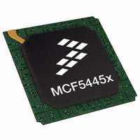
MCF54452VR266 Freescale Semiconductor, MCF54452VR266 Datasheet - Page 23

MCF54452VR266
Manufacturer Part Number
MCF54452VR266
Description
IC MPU 32BIT 266MHZ 360TEPBGA
Manufacturer
Freescale Semiconductor
Series
MCF5445xr
Datasheet
1.MCF54452CVR200.pdf
(48 pages)
Specifications of MCF54452VR266
Core Processor
Coldfire V4
Core Size
32-Bit
Speed
266MHz
Connectivity
I²C, SPI, SSI, UART/USART, USB OTG
Peripherals
DMA, WDT
Number Of I /o
132
Program Memory Type
ROMless
Ram Size
32K x 8
Voltage - Supply (vcc/vdd)
1.35 V ~ 3.6 V
Oscillator Type
Internal
Operating Temperature
0°C ~ 70°C
Package / Case
360-TEPBGA
Family Name
MCF5445X
Device Core
ColdFire
Device Core Size
32b
Frequency (max)
266MHz
Instruction Set Architecture
RISC
Supply Voltage 1 (typ)
3.3V
Operating Supply Voltage (max)
1.65/3.6V
Operating Supply Voltage (min)
1.35/3V
Operating Temp Range
0C to 70C
Operating Temperature Classification
Commercial
Mounting
Surface Mount
Pin Count
360
Package Type
TEBGA
Leaded Process Compatible
Yes
Rohs Compliant
Yes
Peak Reflow Compatible (260 C)
Yes
For Use With
M54455EVB - BOARD EVAL FOR MCF5445X
Lead Free Status / RoHS Status
Lead free / RoHS Compliant
Eeprom Size
-
Program Memory Size
-
Data Converters
-
Lead Free Status / Rohs Status
Compliant
Available stocks
Company
Part Number
Manufacturer
Quantity
Price
Company:
Part Number:
MCF54452VR266
Manufacturer:
Freescale Semiconductor
Quantity:
135
Company:
Part Number:
MCF54452VR266
Manufacturer:
FREESCAL
Quantity:
329
5.7
A multi-function external bus interface called FlexBus is provided with basic functionality to interface to slave-only devices up
to a maximum bus frequency of 66MHz. It can be directly connected to asynchronous or synchronous devices such as external
boot ROMs, flash memories, gate-array logic, or other simple target (slave) devices with little or no additional circuitry. For
asynchronous devices, a simple chip-select based interface can be used.
All processor bus timings are synchronous; input setup/hold and output delay are given in respect to the rising edge of a
reference clock, FB_CLK. The FB_CLK frequency may be the same as the internal system bus frequency or an integer divider
of that frequency.
The following timing numbers indicate when data is latched or driven onto the external bus, relative to the Flexbus output clock
(FB_CLK). All other timing relationships can be derived from these values.
Freescale Semiconductor
1
2
Configuration Overrides*:
FlexBus Timing Specifications
Num
FB1
FB2
FB3
FB4
FB5
Specification is valid for all FB_AD[31:0], FB_BS[3:0], FB_CS[3:0], FB_OE, FB_R/W, FB_TBST,
FB_TSIZ[1:0], and FB_TS.
Specification is valid for all FB_AD[31:0] and FB_TA.
(BOOTMOD[1:0],
The processor drives the data lines during the first clock cycle of the transfer
with the full 32-bit address. This may be ignored by standard connected
devices using non-multiplexed address and data buses. However, some
applications may find this feature beneficial.
The address and data busses are muxed between the FlexBus and PCI
controller. At the end of the read and write bus cycles the address signals are
indeterminate.
Override pins])
Frequency of Operation
Clock Period
Output Valid
Output Hold
Input Setup
Input Hold
RSTOUT
RESET
CLKIN
Figure 8. RESET and Configuration Override Timing
MCF5445x ColdFire
Table 12. FlexBus AC Timing Specifications
R1
Characteristic
R3
®
Microprocessor Data Sheet, Rev. 6
NOTE
R2
R4
Min
1.0
3.0
25
15
—
0
R5
66.66
Max
7.0
40
—
—
—
R6
MHz
Unit
Electrical Characteristics
ns
ns
ns
ns
ns
R4
R7
Notes
1
2
1
2
R8
23


