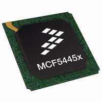
MCF54452VR266 Freescale Semiconductor, MCF54452VR266 Datasheet - Page 27

MCF54452VR266
Manufacturer Part Number
MCF54452VR266
Description
IC MPU 32BIT 266MHZ 360TEPBGA
Manufacturer
Freescale Semiconductor
Series
MCF5445xr
Datasheet
1.MCF54452CVR200.pdf
(48 pages)
Specifications of MCF54452VR266
Core Processor
Coldfire V4
Core Size
32-Bit
Speed
266MHz
Connectivity
I²C, SPI, SSI, UART/USART, USB OTG
Peripherals
DMA, WDT
Number Of I /o
132
Program Memory Type
ROMless
Ram Size
32K x 8
Voltage - Supply (vcc/vdd)
1.35 V ~ 3.6 V
Oscillator Type
Internal
Operating Temperature
0°C ~ 70°C
Package / Case
360-TEPBGA
Family Name
MCF5445X
Device Core
ColdFire
Device Core Size
32b
Frequency (max)
266MHz
Instruction Set Architecture
RISC
Supply Voltage 1 (typ)
3.3V
Operating Supply Voltage (max)
1.65/3.6V
Operating Supply Voltage (min)
1.35/3V
Operating Temp Range
0C to 70C
Operating Temperature Classification
Commercial
Mounting
Surface Mount
Pin Count
360
Package Type
TEBGA
Leaded Process Compatible
Yes
Rohs Compliant
Yes
Peak Reflow Compatible (260 C)
Yes
For Use With
M54455EVB - BOARD EVAL FOR MCF5445X
Lead Free Status / RoHS Status
Lead free / RoHS Compliant
Eeprom Size
-
Program Memory Size
-
Data Converters
-
Lead Free Status / Rohs Status
Compliant
Available stocks
Company
Part Number
Manufacturer
Quantity
Price
Company:
Part Number:
MCF54452VR266
Manufacturer:
Freescale Semiconductor
Quantity:
135
Company:
Part Number:
MCF54452VR266
Manufacturer:
FREESCAL
Quantity:
329
5.9
The PCI bus on the device is PCI 2.2 compliant. The following timing numbers are mostly from the PCI 2.2 spec. Refer to the
PCI 2.2 spec for a more detailed timing analysis.
Freescale Semiconductor
Num
P1
P2
P3
P4
P5
Frequency of Operation
Clock Period
Bused PCI signals — input setup
PCI_GNT[3:0]/PCI_REQ[3:0] — input setup
All PCI signals — input hold
Bused PCI signals — output valid
SD_DQS3/SD_DQS2
SD_DQS3/SD_DQS2
PCI Bus Timing Specifications
D[31:24]/D[23:16]
SD_RAS, SD_CAS
SD_CSn,SD_WE,
D[31:24]/D[23:16]
SD_A[13:0]
SD_CLK
SD_CLK
MCF5445x ColdFire
DD4
Characteristic
Table 14. PCI Timing Specifications
ROW
CMD
Figure 12. DDR Read Timing
DD1
®
DD5
Microprocessor Data Sheet, Rev. 6
COL
CL=2
CL=2.5
DD2
DQS Read
Preamble
DD10
10.0
1
Min
7.0
30
—
—
,
0
2
DQS Read
33 MHz
DD3
Preamble
33.33
Max
11.0
WD1 WD2 WD3 WD4
3
—
—
—
—
WD1 WD2 WD3 WD4
DD9
Electrical Characteristics
33.33
Min
3.0
5.0
15
—
0
66 MHz
DQS Read
Postamble
66.66
Max
6.0
30
3
—
—
—
DQS Read
Postamble
MHz
Unit
ns
ns
ns
ns
ns
27


