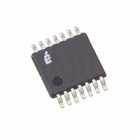
X5329V14T1 Intersil, X5329V14T1 Datasheet - Page 12

X5329V14T1
Manufacturer Part Number
X5329V14T1
Description
IC SUPERVISOR CPU 32K EE 14TSSOP
Manufacturer
Intersil
Type
Simple Reset/Power-On Resetr
Datasheet
1.X5328PZ.pdf
(21 pages)
Specifications of X5329V14T1
Number Of Voltages Monitored
1
Output
Open Drain or Open Collector
Reset
Active High
Reset Timeout
100 ms Minimum
Voltage - Threshold
4.38V
Operating Temperature
0°C ~ 70°C
Mounting Type
Surface Mount
Package / Case
14-TSSOP
Lead Free Status / RoHS Status
Contains lead / RoHS non-compliant
ABSOLUTE MAXIMUM RATINGS
Temperature under bias .................... -65°C to +135°C
Storage temperature ........................ -65°C to +150°C
Voltage on any pin with
D.C. output current ............................................... 5mA
Lead temperature (soldering, 10s) .................... 300°C
D.C. OPERATING CHARACTERISTICS (Over the recommended operating conditions unless otherwise specified.)
CAPACITANCE T
Notes: (1) V
Symbol
RECOMMENDED OPERATING CONDITIONS
respect to V
Symbol
V
V
V
V
V
V
C
V
V
V
I
I
Temperature
I
I
C
CC1
CC2
IH
IL
OH1
OH2
OH3
I
OL1
OL2
OL3
OLS
SB
LO
OUT
Commercial
LI
IN
(1)
(1)
Industrial
(2) This parameter is periodically sampled and not 100% tested.
(2)
(2)
IL
V
V
V
Input Leakage Current
Output Leakage Current
Input LOW Voltage
Input HIGH Voltage
Output LOW Voltage
Output LOW Voltage
Output LOW Voltage
Output HIGH Voltage
Output HIGH Voltage
Output HIGH Voltage
Reset Output LOW Voltage
min. and V
CC
CC
CC
Output Capacitance (SO, RESET, RESET)
Input Capacitance (SCK, SI, CS, WP)
SS
Write Current (Active)
Read Current (Active)
Standby Current
...................................... -1.0V to +7V
A
Parameter
= +25°C, f = 1MHz, V
IH
max. are for reference only and are not tested.
-40°C
12
Min.
0°C
Test
V
V
V
V
CC
CC
CC
CC
CC
Min.
+85°C
-0.5
Max.
70°C
= 5V
x 0.7
- 0.8
- 0.4
- 0.2
X5328, X5329
Limits
Typ.
0.1
0.1
V
V
CC
CC
Max.
0.4
0.4
0.4
0.4
0.4
COMMENT
Stresses above those listed under “Absolute Maximum
Ratings” may cause permanent damage to the device.
This is a stress rating only; functional operation of the
device (at these or any other conditions above those
listed in the operational sections of this specification) is
not implied. Exposure to absolute maximum rating con-
ditions for extended periods may affect device reliability.
10
10
5
1
+ 0.5
x 0.3
Voltage Option
BLank or -4.5A
-2.7 or -2.7A
Unit
Max.
mA
mA
µA
µA
µA
V
V
V
V
V
V
V
V
V
8
6
SO = Open
SO = Open
CS = V
V
V
V
V
V
V
2V < V
V
I
SCK = V
SCK = V
2V < V
OL
CC
IN
OUT
CC
CC
CC
CC
= 1mA
= V
= 5.5V
> 3.3V, I
≤
> 3.3V, I
≤
= V
CC
CC
2V, I
2V, I
CC
SS
CC
CC
SS
, V
Unit
≤
≤
to V
pF
pF
Test Conditions
OL
OH
x 0.1/V
x 0.1/V
3.3V, I
3.3V, I
to V
IN
OL
OH
CC
= 0.5mA
Supply Voltage
= -0.25mA
= V
= 2.1mA
CC
= -1.0mA
2.7V to 5.5V
4.5V-5.5V
SS
OL
OH
CC
CC
or V
= 1mA
= -0.4mA
x 0.9 @ 2MHz,
x 0.9 @ 2MHz,
Conditions
CC
V
V
OUT
IN
,
October 17, 2005
= 0V
= 0V
FN8132.1


