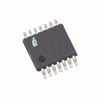
X5329V14T1 Intersil, X5329V14T1 Datasheet - Page 9

X5329V14T1
Manufacturer Part Number
X5329V14T1
Description
IC SUPERVISOR CPU 32K EE 14TSSOP
Manufacturer
Intersil
Type
Simple Reset/Power-On Resetr
Datasheet
1.X5328PZ.pdf
(21 pages)
Specifications of X5329V14T1
Number Of Voltages Monitored
1
Output
Open Drain or Open Collector
Reset
Active High
Reset Timeout
100 ms Minimum
Voltage - Threshold
4.38V
Operating Temperature
0°C ~ 70°C
Mounting Type
Surface Mount
Package / Case
14-TSSOP
Lead Free Status / RoHS Status
Contains lead / RoHS non-compliant
Read Sequence
When reading from the EEPROM memory array, CS is
first pulled low to select the device. The 8-bit READ
instruction is transmitted to the device, followed by the
16-bit address. After the READ opcode and address
are sent, the data stored in the memory at the selected
address is shifted out on the SO line. The data stored
in memory at the next address can be read sequen-
tially by continuing to provide clock pulses. The
address is automatically incremented to the next
higher address after each byte of data is shifted out.
When the highest address is reached, the address
counter rolls over to address $0000 allowing the read
cycle to be continued indefinitely. The read operation
is terminated by taking CS high. Refer to the Read
EEPROM Array Sequence (Figure 1).
To read the Status Register, the CS line is first pulled
low to select the device followed by the 8-bit RDSR
instruction. After the RDSR opcode is sent, the contents
of the Status Register are shifted out on the SO line.
Refer to the Read Status Register Sequence (Figure 2).
Write Sequence
Prior to any attempt to write data into the device, the
“Write Enable” Latch (WEL) must first be set by issu-
ing the WREN instruction (Figure 3). CS is first taken
LOW, then the WREN instruction is clocked into the
device. After all eight bits of the instruction are trans-
mitted, CS must then be taken HIGH. If the user con-
tinues the Write Operation without taking CS HIGH
after issuing the WREN instruction, the Write Opera-
tion will be ignored.
To write data to the EEPROM memory array, the user
then issues the WRITE instruction followed by the
16-bit address and then the data to be written. Any
unused address bits are specified to be “0’s”. The
WRITE operation minimally takes 32 clocks. CS must
go low and remain low for the duration of the opera-
tion. If the address counter reaches the end of a page
and the clock continues, the counter will roll back to
the first address of the page and overwrite any data
that may have been previously written.
9
X5328, X5329
For the Page Write Operation (byte or page write) to
be completed, CS can only be brought HIGH after bit 0
of the last data byte to be written is clocked in. If it is
brought HIGH at any other time, the write operation
will not be completed (Figure 4).
To write to the Status Register, the WRSR instruction
is followed by the data to be written (Figure 5). Data
bits 0 and 1 must be “0”.
While the write is in progress following a Status Regis-
ter or EEPROM Sequence, the Status Register may
be read to check the WIP bit. During this time the WIP
bit will be high.
OPERATIONAL NOTES
The device powers-up in the following state:
– The device is in the low power standby state.
– A HIGH to LOW transition on CS is required to enter
– SO pin is high impedance.
– The Write Enable Latch is reset.
– The Flag Bit is reset.
– Reset Signal is active for t
Data Protection
The following circuitry has been included to prevent
inadvertent writes:
– A WREN instruction must be issued to set the Write
– CS must come HIGH at the proper clock count in
an active state and receive an instruction.
Enable Latch.
order to start a nonvolatile write cycle.
PURST
.
October 17, 2005
FN8132.1


