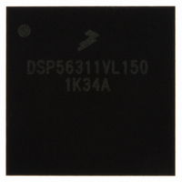
DSP56311VL150 Freescale Semiconductor, DSP56311VL150 Datasheet - Page 18

DSP56311VL150
Manufacturer Part Number
DSP56311VL150
Description
IC DSP 24BIT FIXED POINT 196-BGA
Manufacturer
Freescale Semiconductor
Series
DSP563xxr
Type
Fixed Pointr
Datasheet
1.DSP56311VL150R2.pdf
(96 pages)
Specifications of DSP56311VL150
Interface
Host Interface, SSI, SCI
Clock Rate
150MHz
Non-volatile Memory
ROM (576 B)
On-chip Ram
384kB
Voltage - I/o
3.30V
Voltage - Core
1.80V
Operating Temperature
-40°C ~ 100°C
Mounting Type
Surface Mount
Package / Case
196-MAPBGA
Package
196MA-BGA
Numeric And Arithmetic Format
Fixed-Point
Maximum Speed
150 MHz
Ram Size
384 KB
Device Million Instructions Per Second
150 MIPS
Lead Free Status / RoHS Status
Lead free / RoHS Compliant
Available stocks
Company
Part Number
Manufacturer
Quantity
Price
Company:
Part Number:
DSP56311VL150
Manufacturer:
FREESCALE
Quantity:
201
Company:
Part Number:
DSP56311VL150
Manufacturer:
MOTOLOLA
Quantity:
1 045
Company:
Part Number:
DSP56311VL150
Manufacturer:
Freescale Semiconductor
Quantity:
10 000
Part Number:
DSP56311VL150
Manufacturer:
FREESCALE
Quantity:
20 000
Company:
Part Number:
DSP56311VL150B1
Manufacturer:
ST
Quantity:
101
Company:
Part Number:
DSP56311VL150B1
Manufacturer:
Freescale Semiconductor
Quantity:
10 000
Company:
Part Number:
DSP56311VL150R2
Manufacturer:
Freescale Semiconductor
Quantity:
10 000
Signals/Connections
1.11 Timers
The DSP56311 has three identical and independent timers. Each timer can use internal or external clocking and can
either interrupt the DSP56311 after a specified number of events (clocks) or signal an external device after
counting a specific number of internal events.
1-14
SCLK
PE2
Notes:
TIO0
TIO1
TIO2
Notes:
Signal Name
Signal Name
1.
2.
1.
2.
In the Stop state, the signal maintains the last state as follows:
• If the last state is input, the signal is an ignored input.
• If the last state is output, these lines have weak keepers that maintain the last output state even if the drivers are tri-stated.
The Wait processing state does not affect the signal state.
Input/Output
Input or Output
Input or Output
Input or Output
Input or Output
Type
Type
Table 1-14.
Ignored Input
Ignored Input
Ignored Input
State During
State During
Ignored Input
Reset
Reset
Table 1-15.
DSP56311 Technical Data, Rev. 8
Serial Communication Interface (Continued)
1,2
1,2
Serial Clock—Provides the input or output clock used by the transmitter and/or
the receiver.
Port E 2—The default configuration following reset is GPIO input PE2. When
configured as PE2, signal direction is controlled through the Port E Direction
Register. The signal can be configured as an SCI signal SCLK through the Port
E Control Register.
Timer 0 Schmitt-Trigger Input/Output— When Timer 0 functions as an
external event counter or in measurement mode, TIO0 is used as input. When
Timer 0 functions in watchdog, timer, or pulse modulation mode, TIO0 is used
as output.
The default mode after reset is GPIO input. TIO0 can be changed to output or
configured as a timer I/O through the Timer 0 Control/Status Register (TCSR0).
Timer 1 Schmitt-Trigger Input/Output— When Timer 1 functions as an
external event counter or in measurement mode, TIO1 is used as input. When
Timer 1 functions in watchdog, timer, or pulse modulation mode, TIO1 is used
as output.
The default mode after reset is GPIO input. TIO1 can be changed to output or
configured as a timer I/O through the Timer 1 Control/Status Register (TCSR1).
Timer 2 Schmitt-Trigger Input/Output— When Timer 2 functions as an
external event counter or in measurement mode, TIO2 is used as input. When
Timer 2 functions in watchdog, timer, or pulse modulation mode, TIO2 is used
as output.
The default mode after reset is GPIO input. TIO2 can be changed to output or
configured as a timer I/O through the Timer 2 Control/Status Register (TCSR2).
Triple Timer Signals
Signal Description
Signal Description
Freescale Semiconductor


