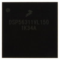
DSP56311VL150 Freescale Semiconductor, DSP56311VL150 Datasheet - Page 57

DSP56311VL150
Manufacturer Part Number
DSP56311VL150
Description
IC DSP 24BIT FIXED POINT 196-BGA
Manufacturer
Freescale Semiconductor
Series
DSP563xxr
Type
Fixed Pointr
Datasheet
1.DSP56311VL150R2.pdf
(96 pages)
Specifications of DSP56311VL150
Interface
Host Interface, SSI, SCI
Clock Rate
150MHz
Non-volatile Memory
ROM (576 B)
On-chip Ram
384kB
Voltage - I/o
3.30V
Voltage - Core
1.80V
Operating Temperature
-40°C ~ 100°C
Mounting Type
Surface Mount
Package / Case
196-MAPBGA
Package
196MA-BGA
Numeric And Arithmetic Format
Fixed-Point
Maximum Speed
150 MHz
Ram Size
384 KB
Device Million Instructions Per Second
150 MIPS
Lead Free Status / RoHS Status
Lead free / RoHS Compliant
Available stocks
Company
Part Number
Manufacturer
Quantity
Price
Company:
Part Number:
DSP56311VL150
Manufacturer:
FREESCALE
Quantity:
201
Company:
Part Number:
DSP56311VL150
Manufacturer:
MOTOLOLA
Quantity:
1 045
Company:
Part Number:
DSP56311VL150
Manufacturer:
Freescale Semiconductor
Quantity:
10 000
Part Number:
DSP56311VL150
Manufacturer:
FREESCALE
Quantity:
20 000
Company:
Part Number:
DSP56311VL150B1
Manufacturer:
ST
Quantity:
101
Company:
Part Number:
DSP56311VL150B1
Manufacturer:
Freescale Semiconductor
Quantity:
10 000
Company:
Part Number:
DSP56311VL150R2
Manufacturer:
Freescale Semiconductor
Quantity:
10 000
2.4.10.2 With an Operating Frequency above 100 MHz
The following considerations can be helpful when GPIO is used for output or input with an operating frequency
above 100 MHz (that is, when
2.4.11 JTAG Timing
Freescale Semiconductor
Notes:
No.
500
501
502
503
504
505
506
507
508
509
510
511
512
513
•
•
GPIO as Output:
— The time from fetch of the instruction that changes the GPIO pin to the actual change is seven core
— The maximum rise or fall time of a GPIO pin is 13 ns (TTL levels, assuming that the maximum of 50
GPIO as Input—GPIO inputs are not synchronized with the core clock. When only one GPIO bit is polled,
this lack of synchronization presents no problem, since the read value can be either the previous value or
the new value of the corresponding GPIO pin. However, there is the risk of reading an intermediate state if:
— Two or more GPIO bits are treated as a coupled group (for example, four possible status states encoded
— The read operation occurs during a simultaneous change of GPIO pins (for example, the change of 00
Therefore, when GPIO bits are read, the recommended practice is to poll continuously until two
consecutive read operations have identical results.
1.
2.
TCK frequency of operation (1/(T
TCK cycle time in Crystal mode
TCK clock pulse width measured at 1.5 V
TCK rise and fall times
Boundary scan input data set-up time
Boundary scan input data hold time
TCK low to output data valid
TCK low to output high impedance
TMS, TDI data set-up time
TMS, TDI data hold time
TCK low to TDO data valid
TCK low to TDO high impedance
TRST assert time
TRST set-up time to TCK low
clock cycles. This is true, assuming that the instruction is a on
pipeline stalls or any other pipeline delays.
pF load limit is met).
in two bits).
to 11 may happen through an intermediate state of 01 or 10).
V
All timings apply to OnCE module data transfers because it uses the JTAG port as an interface.
CCQH
= 3.3 V ± 0.3 V, V
CLKOUT
CC
= 1.8 V ± 0.1 V; T
Characteristics
C
× 3); maximum 22 MHz)
is not available).
DSP56311 Technical Data, Rev. 8
Table 2-19.
J
= –40°C to +100 °C, C
JTAG Timing
L
= 50 pF.
e
-cycle instruction and that there are no
100.0
Min
45.0
20.0
24.0
25.0
40.0
0.0
0.0
5.0
0.0
0.0
5.0
0.0
0.0
All frequencies
AC Electrical Characteristics
Max
22.0
40.0
40.0
44.0
44.0
3.0
—
—
—
—
—
—
—
—
Unit
MHz
ns
ns
ns
ns
ns
ns
ns
ns
ns
ns
ns
ns
ns
2-37


