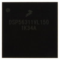
DSP56311VL150 Freescale Semiconductor, DSP56311VL150 Datasheet - Page 50

DSP56311VL150
Manufacturer Part Number
DSP56311VL150
Description
IC DSP 24BIT FIXED POINT 196-BGA
Manufacturer
Freescale Semiconductor
Series
DSP563xxr
Type
Fixed Pointr
Datasheet
1.DSP56311VL150R2.pdf
(96 pages)
Specifications of DSP56311VL150
Interface
Host Interface, SSI, SCI
Clock Rate
150MHz
Non-volatile Memory
ROM (576 B)
On-chip Ram
384kB
Voltage - I/o
3.30V
Voltage - Core
1.80V
Operating Temperature
-40°C ~ 100°C
Mounting Type
Surface Mount
Package / Case
196-MAPBGA
Package
196MA-BGA
Numeric And Arithmetic Format
Fixed-Point
Maximum Speed
150 MHz
Ram Size
384 KB
Device Million Instructions Per Second
150 MIPS
Lead Free Status / RoHS Status
Lead free / RoHS Compliant
Available stocks
Company
Part Number
Manufacturer
Quantity
Price
Company:
Part Number:
DSP56311VL150
Manufacturer:
FREESCALE
Quantity:
201
Company:
Part Number:
DSP56311VL150
Manufacturer:
MOTOLOLA
Quantity:
1 045
Company:
Part Number:
DSP56311VL150
Manufacturer:
Freescale Semiconductor
Quantity:
10 000
Part Number:
DSP56311VL150
Manufacturer:
FREESCALE
Quantity:
20 000
Company:
Part Number:
DSP56311VL150B1
Manufacturer:
ST
Quantity:
101
Company:
Part Number:
DSP56311VL150B1
Manufacturer:
Freescale Semiconductor
Quantity:
10 000
Company:
Part Number:
DSP56311VL150R2
Manufacturer:
Freescale Semiconductor
Quantity:
10 000
Specifications
2.4.7
2-30
Notes:
No.
400
401
402
403
404
405
406
407
408
409
410
411
412
413
414
415
Synchronous clock cycle
Clock low period
Clock high period
Output data set-up to clock falling edge (internal
clock)
Output data hold after clock rising edge (internal
clock)
Input data set-up time before clock rising edge
(internal clock)
Input data not valid before clock rising edge
(internal clock)
Clock falling edge to output data valid (external
clock)
Output data hold after clock rising edge (external
clock)
Input data set-up time before clock rising edge
(external clock)
Input data hold time after clock rising edge
(external clock)
Asynchronous clock cycle
Clock low period
Clock high period
Output data set-up to clock rising edge (internal
clock)
Output data hold after clock rising edge (internal
clock)
1.
2.
3.
SCI Timing
V
t
t
control register and T
SCC
ACC
CCQH
= synchronous clock cycle time (for internal clock, t
= asynchronous clock cycle time; value given for 1X Clock mode (for internal clock, t
= 3.3 V ± 0.3 V, V
Characteristics
C
).
CC
1
= 1.8 V ± 0.1 V; T
DSP56311 Technical Data, Rev. 8
Table 2-15.
J
= –40°C to +100 °C, C
Symbol
t
t
SCC
ACC
2
3
SCC
SCI Timings
is determined by the SCI clock control register and T
t
t
SCC
t
SCC
SCC
t
SCC
/4 + 0.5 × T
/4 + 0.5 × T
Expression
/4 + 0.5 × T
L
t
t
t
t
t
t
SCC
SCC
ACC
ACC
ACC
ACC
= 50 pF
T
64 × T
/4 − 0.5 × T
8 × T
C
/2 − 10.0
/2 − 10.0
/2 − 10.0
/2 − 10.0
/2 − 30.0
/2 − 30.0
+ 8.0
C
C
C
C
C
+ 25.0
− 10.0
− 5.5
C
ACC
is determined by the SCI clock
427.0
203.5
203.5
183.5
183.5
Freescale Semiconductor
Min
53.3
16.7
16.7
10.0
41.7
14.7
6.7
0.0
9.0
—
—
150 MHz
Max
11.5
32.0
—
—
—
—
—
—
—
—
—
—
—
—
—
—
C
).
Unit
ns
ns
ns
ns
ns
ns
ns
ns
ns
ns
ns
ns
ns
ns
ns
ns


