ATA5760N-TGSY Atmel, ATA5760N-TGSY Datasheet - Page 16

ATA5760N-TGSY
Manufacturer Part Number
ATA5760N-TGSY
Description
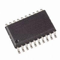
IC RCVR UHF ASKFSK 868MHZ 20SOIC
Manufacturer
Atmel
Datasheet
1.ATA5760N-TGSY.pdf
(41 pages)
Specifications of ATA5760N-TGSY
Frequency
868MHz
Sensitivity
-110dBm
Data Rate - Maximum
10 kBaud
Modulation Or Protocol
ASK, FSK
Applications
Telemetering and Security Systems
Current - Receiving
7.8mA
Data Interface
PCB, Surface Mount
Antenna Connector
PCB, Surface Mount
Voltage - Supply
4.5 V ~ 5.5 V
Operating Temperature
-40°C ~ 105°C
Package / Case
20-SOIC (0.300", 7.50mm Width)
Lead Free Status / RoHS Status
Lead free / RoHS Compliant
Features
-
Memory Size
-
8.7
Figure 8-10. Timing Diagram of the OFF Command via Pin DATA
Figure 8-11. Timing Diagram of the OFF Command via Pin POLLING/_ON
16
Switching the Receiver Back to Sleep Mode
Serial bi-directional
data line
Data_out (DATA)
Out1
(microcontroller)
IC_ACTIVE
ATA5760/ATA5761
IC_ACTIVE
POLLING/_ON
Data_out (DATA)
Serial bi-directional
data line
X
X
The receiver can be set back to polling mode via pin DATA or via pin POLLING/_ON.
When using pin DATA, this pin must be pulled to Low for the period t1 by the connected micro-
controller.
on page
limited but it is recommended not to exceed the specified value to prevent erasing the reset
marker. Note also that an internal reset for the OPMODE and the LIMIT register will be gener-
ated if t1 exceeds the specified values. This item is explained in more detail in the section
“Configuration of the Receiver” on page
achieved by programming bit 1 to be ‘1’ during the register configuration. Only one sync pulse
(t3) is issued.
The duration of the OFF command is determined by the sum of t1, t2 and t10. After the OFF
command the sleep time T
section
Receiving
mode
t1
Receiving mode
“Data Interface” on page
28). The minimum value of t1 depends on BR_Range. The maximum value for t1 is not
Figure 8-10 on page 16
X
X
OFF-command
t2
t
on2
t3
(Start bit)
t4
Bit 1
("1")
Sleep mode
t
on3
t10
t5
t7
Sleep
elapses. Note that the capacitive load at pin DATA is limited (see
29).
illustrates the timing of the OFF command (see
Start-up mode
23. Setting the receiver to sleep mode via DATA is
Sleep mode
Bit-check mode
T
Sleep
Bit check ok
X
X
Receiving mode
Start-up mode
T
Start-up
4896D–RKE–08/08
Figure 13-2


