AC4486-5M Laird Technologies, AC4486-5M Datasheet - Page 4
AC4486-5M
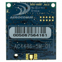
Manufacturer Part Number
AC4486-5M
Description
TXRX 868MHZ 3V TTL 5MW RS232
Manufacturer
Laird Technologies
Series
AeroCommr
Specifications of AC4486-5M
Frequency
868MHz
Data Rate - Maximum
115.2kbps
Modulation Or Protocol
FSK
Applications
AMR, Gaming Devices, Inventory Tracking
Power - Output
5mW
Sensitivity
-100dBm
Voltage - Supply
3.3V
Current - Receiving
30mA
Current - Transmitting
40mA
Data Interface
Connector, 2 x 10 Header
Antenna Connector
MMCX
Operating Temperature
-40°C ~ 85°C
Package / Case
Module
Board Size
49 mm x 42 mm x 5 mm
Output Power
5 mW
Antenna
External MMCX Connector
Frequency Rf
869.65MHz
Transmit Power
5mW
Interface Type
Serial
Rohs Compliant
Yes
Lead Free Status / RoHS Status
Lead free / RoHS Compliant
Memory Size
-
Lead Free Status / Rohs Status
Lead free / RoHS Compliant
Available stocks
Company
Part Number
Manufacturer
Quantity
Price
Company:

Part Number:
AC4486-5M
Manufacturer:
Laird Technologies Wireless M2
Quantity:
135


1.
2.
3.
3.1
3.2
3.3
4.
4.1
4.2
4.3
4.4
4.5
4.6
01/21/05
TABLE OF CONTENTS
3.3.1
3.3.2
3.3.3
3.3.4
4.4.1
4.4.2
4.4.3
4.5.1
4.5.2
4.5.3
4.6.1
4.6.2
4.6.3
4.6.4
4.6.5
4.6.6
4.6.7
4.6.8
4.6.9
4.6.10
4.6.11
4.6.12
4.6.13
4.6.14
4.6.15
4.6.16
4.6.17
4.6.18
4.6.19
4.6.20
4.6.21
4.6.22
4.6.23
4.6.24
4.6.25
4.6.26
OVERVIEW ......................................................................................................................................7
AC4486 SPECIFICATIONS ............................................................................................................8
SPECIFICATIONS ...........................................................................................................................9
I
E
S
CONFIGURING THE AC4486......................................................................................................15
EEPROM P
C
C
EEPROM C
AC4486 AT C
O
NTERFACE
YSTEM
LECTRICAL
ONFIGURATION FLOW OF THE
OMMAND
N
-
THE
Serial Interface Data Rate .........................................................................................................11
Latency ......................................................................................................................................11
Timing Diagrams.......................................................................................................................12
Maximum Overall System Throughput ......................................................................................14
EEPROM Byte Read..................................................................................................................22
EEPROM Byte Write .................................................................................................................22
EEPROM Exit Configuration Mode Command.........................................................................23
Enter AT Command Mode .........................................................................................................23
AT Enter Configuration Mode ...................................................................................................24
Exit AT Command Mode............................................................................................................24
Status Request............................................................................................................................25
Change Channel without Forced Acquisition Sync ...................................................................25
Change Channel with Forced Acquisition Sync ........................................................................25
Server/Client Command.............................................................................................................26
Sync to Channel Command........................................................................................................26
Sleep Walk Power-Down Command..........................................................................................27
Sleep Walk Power-Down Wake-Up Command..........................................................................27
Broadcast Mode.........................................................................................................................27
Read Static Bank #1 Byte...........................................................................................................28
Write Static Bank #1 Byte ..........................................................................................................28
Read Static Bank #2 Byte...........................................................................................................28
Write Static Bank #2 Byte ..........................................................................................................30
Write Destination Address.........................................................................................................30
Read Destination Address..........................................................................................................30
Auto Destination ........................................................................................................................31
Read Digital Inputs....................................................................................................................31
Read ADC..................................................................................................................................32
Report Last Valid RSSI ..............................................................................................................33
Write Digital Outputs ................................................................................................................34
Write DAC .................................................................................................................................34
Set Max Power...........................................................................................................................35
Transmit Buffer Empty...............................................................................................................35
Disable Sync to Channel............................................................................................................35
Deep Sleep Mode .......................................................................................................................36
Read Temperature .....................................................................................................................36
EEPROM Byte Read..................................................................................................................36
-F
T
IMING AND LATENCY
LY
Q
S
ARAMETERS
ONFIGURATION
S
IGNAL
UICK
C
PECIFICATIONS
OMMANDS
ONTROL
R
D
EFERENCE
EFINITIONS
C
....................................................................................................................15
OMMANDS
...................................................................................................................23
C
.............................................................................................................10
OMMANDS
...........................................................................................................20
AC4486 ............................................................................................19
..........................................................................................................11
.........................................................................................................9
(CC C
...........................................................................................22
OMMAND
M
ODE
) ............................................................24
4
Related parts for AC4486-5M
Image
Part Number
Description
Manufacturer
Datasheet
Request
R

Part Number:
Description:
TXRX 868MHZ 3V TTL 5MW RS232
Manufacturer:
Laird Technologies
Datasheet:

Part Number:
Description:
TXRX 868MHZ 3V TTL 5MW RS485
Manufacturer:
Laird Technologies
Datasheet:
Part Number:
Description:
TXRX 868MHZ 3V TTL 5MW RS485
Manufacturer:
Laird Technologies
Datasheet:

Part Number:
Description:
Bluetooth Serial Module Development Kit
Manufacturer:
Laird Technologies
Part Number:
Description:
BLUETOOTH MODULE DEVELOPMENT KIT
Manufacturer:
Laird Technologies
Part Number:
Description:
Bluetooth 2.0 AT Data Module, Internal Antenna Development Kit
Manufacturer:
Laird Technologies

Part Number:
Description:
BLUETOOTH EVAL BOARD BTM511
Manufacturer:
Laird Technologies
Datasheet:

Part Number:
Description:
Bluetooth / 802.15.1 Modules & Development Tools BLUETTH Multimed MODLE, No ANT DEVKIT
Manufacturer:
Laird Technologies
Datasheet:

Part Number:
Description:
DEV KIT PRM122
Manufacturer:
Laird Technologies
Datasheet:
Part Number:
Description:
DEV KIT PRM123
Manufacturer:
Laird Technologies
Datasheet:

Part Number:
Description:
CHOKE COMMON MODE 110 OHMS SMD
Manufacturer:
Laird Technologies
Datasheet: