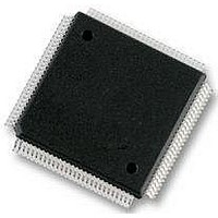
S9S12XS128J1MAL Freescale Semiconductor, S9S12XS128J1MAL Datasheet - Page 555

S9S12XS128J1MAL
Manufacturer Part Number
S9S12XS128J1MAL
Description
IC MCU 16BIT 128KB FLSH 112LQFP
Manufacturer
Freescale Semiconductor
Series
HCS12r
Datasheet
1.MC9S12XS64CAE.pdf
(738 pages)
Specifications of S9S12XS128J1MAL
Core Processor
HCS12X
Core Size
16-Bit
Speed
40MHz
Connectivity
CAN, SCI, SPI
Peripherals
LVD, POR, PWM, WDT
Number Of I /o
91
Program Memory Size
128KB (128K x 8)
Program Memory Type
FLASH
Eeprom Size
8K x 8
Ram Size
8K x 8
Voltage - Supply (vcc/vdd)
1.72 V ~ 5.5 V
Data Converters
A/D 16x12b
Oscillator Type
External
Operating Temperature
-40°C ~ 125°C
Package / Case
112-LQFP
Processor Series
S12XS
Core
HCS12
Data Bus Width
16 bit
Data Ram Size
8 KB
Interface Type
CAN, SCI, SPI
Maximum Clock Frequency
40 MHz
Number Of Programmable I/os
91
Number Of Timers
12
Maximum Operating Temperature
+ 125 C
Mounting Style
SMD/SMT
3rd Party Development Tools
EWHCS12
Development Tools By Supplier
DEMO9S12XSFAME, EVB9S12XEP100
Minimum Operating Temperature
- 40 C
On-chip Adc
12 bit, 16 Channel
Lead Free Status / RoHS Status
Lead free / RoHS Compliant
Available stocks
Company
Part Number
Manufacturer
Quantity
Price
Company:
Part Number:
S9S12XS128J1MAL
Manufacturer:
Freescale Semiconductor
Quantity:
10 000
- Current page: 555 of 738
- Download datasheet (4Mb)
keys stored in the Flash memory via the Memory Controller. If the keys presented in the Verify Backdoor
Access Key command match the backdoor keys stored in the Flash memory, the SEC bits in the FSEC
register (see
not permitted as backdoor keys. While the Verify Backdoor Access Key command is active, P-Flash block
0 will not be available for read access and will return invalid data.
The user code stored in the P-Flash memory must have a method of receiving the backdoor keys from an
external stimulus. This external stimulus would typically be through one of the on-chip serial ports.
If the KEYEN[1:0] bits are in the enabled state (see
backdoor key access sequence described below:
The Verify Backdoor Access Key command is monitored by the Memory Controller and an illegal key will
prohibit future use of the Verify Backdoor Access Key command. A reset of the MCU is the only method
to re-enable the Verify Backdoor Access Key command.
After the backdoor keys have been correctly matched, the MCU will be unsecured. After the MCU is
unsecured, the sector containing the Flash security byte can be erased and the Flash security byte can be
reprogrammed to the unsecure state, if desired.
In the unsecure state, the user has full control of the contents of the backdoor keys by programming
addresses 0x7F_FF00–0x7F_FF07 in the Flash configuration field.
The security as defined in the Flash security byte (0x7F_FF0F) is not changed by using the Verify
Backdoor Access Key command sequence. The backdoor keys stored in addresses
0x7F_FF00–0x7F_FF07 are unaffected by the Verify Backdoor Access Key command sequence. After the
next reset of the MCU, the security state of the Flash module is determined by the Flash security byte
(0x7F_FF0F). The Verify Backdoor Access Key command sequence has no effect on the program and
erase protections defined in the Flash protection register, FPROT.
18.5.2
The MCU can be unsecured in special single chip mode by erasing the P-Flash and D-Flash memory by
one of the following methods:
After the CCIF flag sets to indicate that the Erase All Blocks operation has completed, reset the MCU into
special single chip mode. The BDM will execute the Erase Verify All Blocks command write sequence to
verify that the P-Flash and D-Flash memory is erased. If the P-Flash and D-Flash memory are verified as
Freescale Semiconductor
1. Follow the command sequence for the Verify Backdoor Access Key command as explained in
2. If the Verify Backdoor Access Key command is successful, the MCU is unsecured and the
•
•
Section 18.4.2.11
SEC[1:0] bits in the FSEC register are forced to the unsecure state of 10
Reset the MCU into special single chip mode, delay while the erase test is performed by the BDM,
send BDM commands to disable protection in the P-Flash and D-Flash memory, and execute the
Erase All Blocks command write sequence to erase the P-Flash and D-Flash memory.
Reset the MCU into special expanded wide mode, disable protection in the P-Flash and D-Flash
memory and run code from external memory to execute the Erase All Blocks command write
sequence to erase the P-Flash and D-Flash memory.
Unsecuring the MCU in Special Single Chip Mode using BDM
Table
18-10) will be changed to unsecure the MCU. Key values of 0x0000 and 0xFFFF are
S12XS Family Reference Manual, Rev. 1.11
Section
18.3.2.2), the MCU can be unsecured by the
256 KByte Flash Module (S12XFTMR256K1V1)
555
Related parts for S9S12XS128J1MAL
Image
Part Number
Description
Manufacturer
Datasheet
Request
R
Part Number:
Description:
Manufacturer:
Freescale Semiconductor, Inc
Datasheet:
Part Number:
Description:
Manufacturer:
Freescale Semiconductor, Inc
Datasheet:
Part Number:
Description:
Manufacturer:
Freescale Semiconductor, Inc
Datasheet:
Part Number:
Description:
Manufacturer:
Freescale Semiconductor, Inc
Datasheet:
Part Number:
Description:
Manufacturer:
Freescale Semiconductor, Inc
Datasheet:
Part Number:
Description:
Manufacturer:
Freescale Semiconductor, Inc
Datasheet:
Part Number:
Description:
Manufacturer:
Freescale Semiconductor, Inc
Datasheet:
Part Number:
Description:
Manufacturer:
Freescale Semiconductor, Inc
Datasheet:
Part Number:
Description:
Manufacturer:
Freescale Semiconductor, Inc
Datasheet:
Part Number:
Description:
Manufacturer:
Freescale Semiconductor, Inc
Datasheet:
Part Number:
Description:
Manufacturer:
Freescale Semiconductor, Inc
Datasheet:
Part Number:
Description:
Manufacturer:
Freescale Semiconductor, Inc
Datasheet:
Part Number:
Description:
Manufacturer:
Freescale Semiconductor, Inc
Datasheet:
Part Number:
Description:
Manufacturer:
Freescale Semiconductor, Inc
Datasheet:
Part Number:
Description:
Manufacturer:
Freescale Semiconductor, Inc
Datasheet:


