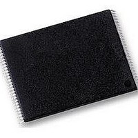
S29GL032N90TFI030 Spansion Inc., S29GL032N90TFI030 Datasheet - Page 17

S29GL032N90TFI030
Manufacturer Part Number
S29GL032N90TFI030
Description
Flash 3V 32Mb Float Gate two address 90s
Manufacturer
Spansion Inc.
Datasheet
1.S29GL032N90TFI010.pdf
(81 pages)
Specifications of S29GL032N90TFI030
Memory Type
NOR
Memory Size
32 Mbit
Access Time
90 ns
Data Bus Width
8 bit, 16 bit
Architecture
Uniform / Boot Sector
Interface Type
Page-mode
Supply Voltage (max)
3.6 V
Supply Voltage (min)
2.7 V
Maximum Operating Current
50 mA
Mounting Style
SMD/SMT
Operating Temperature
+ 85 C
Package / Case
TSOP-48
Ic Interface Type
CFI, Parallel
Supply Voltage Range
2.7V To 3.6V
Memory Case Style
TSOP
No. Of Pins
48
Lead Free Status / RoHS Status
Lead free / RoHS Compliant
Lead Free Status / RoHS Status
Lead free / RoHS Compliant, Lead free / RoHS Compliant
Available stocks
Company
Part Number
Manufacturer
Quantity
Price
Company:
Part Number:
S29GL032N90TFI030
Manufacturer:
SPANSION
Quantity:
6 035
Part Number:
S29GL032N90TFI030
Manufacturer:
SPANSION
Quantity:
20 000
Company:
Part Number:
S29GL032N90TFI030
Manufacturer:
SPANSIO
Quantity:
3 888
Company:
Part Number:
S29GL032N90TFI030H
Manufacturer:
Spansion
Quantity:
1 440
Part Number:
S29GL032N90TFI030H
Manufacturer:
SPANSION
Quantity:
20 000
8. Device Bus Operations
Legend
L = Logic Low = V
H = Logic High = V
V
X = Don’t Care
A
D
D
Notes
1. If WP# = V
2. D
8.1
8.2
October 29, 2008 S29GL-N_01_12
Read
Write (Program/Erase)
Accelerated Program
Standby
Output Disable
Reset
HH
IN
IN
OUT
= VIH, the first or last sector, or the two outer boot sectors are protected or unprotected as determined by the method described in Write Protect (WP#). All
sectors are unprotected when shipped from the factory (The Secured Silicon Sector may be factory protected depending on version ordered.)
= Address In
= Data In
= 11.5–12.5 V
IN
= Data Out
or D
Operation
OUT
Word/Byte Configuration
Requirements for Reading Array Data
IL
, the first or last sector remains protected (for uniform sector devices), and the two outer boot sectors are protected (for boot sector devices). If WP#
as required by command sequence, data polling, or sector protect algorithm (see
IL
IH
This section describes the requirements and use of the device bus operations, which are initiated through the
internal command register. The command register itself does not occupy any addressable memory location.
The register is a latch used to store the commands, along with the address and data information needed to
execute the command. The contents of the register serve as inputs to the internal state machine. The state
machine outputs dictate the function of the device.
control levels they require, and the resulting output. The following subsections describe each of these
operations in further detail.
The BYTE# pin controls whether the device data I/O pins operate in the byte or word configuration. If the
BYTE# pin is set at logic 1, the device is in word configuration, DQ0–DQ15 are active and controlled by CE#,
WE# and OE#.
If the BYTE# pin is set at logic 0, the device is in byte configuration, and only data I/O pins DQ0–DQ7 are
active and controlled by CE#, WE# and OE#. The data I/O pins DQ8–DQ14 are tri-stated, and the DQ15 pin
is used as an input for the LSB (A-1) address function.
All memories require access time to output array data. In a read operation, data is read from one memory
location at a time. Addresses are presented to the device in random order, and the propagation delay through
the device causes the data on its outputs to arrive with the address on its inputs.
The device defaults to reading array data after device power-up or hardware reset. To read data from the
memory array, the system must first assert a valid address on Amax-A0, while driving OE# and CE# to V
WE# must remain at V
DQ15-DQ0 after address access time (t
data. The OE# signal must be driven to V
elapsed from the falling edge of OE#.
See
specifications and the timing diagram. Refer to
reading array data.
Reading Array Data on page 41
V
CC
CE#
± 0.3V
X
L
L
L
L
IH
OE#
H
H
X
H
X
L
. All addresses are latched on the falling edge of CE#. Data will appear on
D a t a
Table 8.1 Device Bus Operations
WE#
S29GL-N MirrorBit
H
X
H
X
L
L
S h e e t
V
RESET#
CC
for more information. Refer to
ACC
H
H
H
± 0.3V
H
L
IL
. Data is output on DQ15-DQ0 pins after the access time (t
), which is equal to the delay from stable addresses to valid output
®
Table 13.1 on page 62
(Note 1)
(Note 1)
Flash Family
WP#
X
X
X
X
Table 8.1
ACC
V
Figure 10.5 on page
X
X
H
X
X
HH
lists the device bus operations, the inputs and
Addresses
Table 15.1 on page 64
A
A
A
X
X
X
IN
IN
IN
for the active current specification on
56).
(Note 2)
(Note 2)
High-Z
High-Z
High-Z
DQ0–
D
DQ7
OUT
(Note 2)
(Note 2)
BYTE#
High-Z
High-Z
High-Z
D
= V
OUT
for timing
IH
DQ8–DQ15
DQ15 = A-1
DQ8–DQ14
= High-Z,
BYTE#
High-Z
High-Z
High-Z
= V
OE
IL
) has
IL
17
.


