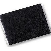
S29GL032N90TFI030 Spansion Inc., S29GL032N90TFI030 Datasheet - Page 64

S29GL032N90TFI030
Manufacturer Part Number
S29GL032N90TFI030
Description
Flash 3V 32Mb Float Gate two address 90s
Manufacturer
Spansion Inc.
Datasheet
1.S29GL032N90TFI010.pdf
(81 pages)
Specifications of S29GL032N90TFI030
Memory Type
NOR
Memory Size
32 Mbit
Access Time
90 ns
Data Bus Width
8 bit, 16 bit
Architecture
Uniform / Boot Sector
Interface Type
Page-mode
Supply Voltage (max)
3.6 V
Supply Voltage (min)
2.7 V
Maximum Operating Current
50 mA
Mounting Style
SMD/SMT
Operating Temperature
+ 85 C
Package / Case
TSOP-48
Ic Interface Type
CFI, Parallel
Supply Voltage Range
2.7V To 3.6V
Memory Case Style
TSOP
No. Of Pins
48
Lead Free Status / RoHS Status
Lead free / RoHS Compliant
Lead Free Status / RoHS Status
Lead free / RoHS Compliant, Lead free / RoHS Compliant
Available stocks
Company
Part Number
Manufacturer
Quantity
Price
Company:
Part Number:
S29GL032N90TFI030
Manufacturer:
SPANSION
Quantity:
6 035
Part Number:
S29GL032N90TFI030
Manufacturer:
SPANSION
Quantity:
20 000
Company:
Part Number:
S29GL032N90TFI030H
Manufacturer:
Spansion
Quantity:
1 440
Part Number:
S29GL032N90TFI030H
Manufacturer:
SPANSION
Quantity:
20 000
15. AC Characteristics
Notes
1. Not 100% tested.
2. See
64
JEDEC
t
t
t
t
t
t
t
GLQV
EHQZ
GHQZ
AXQX
AVQV
ELQV
AVAV
Parameter
Figure 14.1 on page 63
t
RESET#
t
Std.
t
PACC
t
ACC
t
t
t
OEH
t
t
RC
CE
OE
DF
DF
OH
V
CE#
CC
Read Cycle Time
Address to Output Delay
Chip Enable to Output Delay
Page Access Time
Output Enable to Output Delay
Chip Enable to Output High Z
Output Enable to Output High Z
Output Hold Time From Addresses, CE# or OE#,
Whichever Occurs First
Output Enable Hold
Time
(Note 1)
and
Table 14.1 on page 63
(Note 1)
Description
Read
Toggle and
Data# Polling
Figure 15.1 V
Table 15.1 Read-Only Operations
for test specifications.
S29GL-N MirrorBit
(Note 1)
(Note 1)
V
CC
min
CC
t
VCS
D a t a
Power-up Diagram
®
Flash Family
V
V
V
S h e e t
IO
IO
IH
V
V
CE#, OE# = V
= 1.8 V, V
= 1.8 V, V
IO
IO
OE# = V
= V
= V
Test Setup
CC
CC
CC
CC
= 3 V
= 3 V
IL
t
RH
= 3 V
= 3 V
IL
S29GL-N_01_12 October 29, 2008
Max
Max
Max
Max
Max
Max
Min
Min
Min
Min
Speed Options
90
90
90
90
25
—
25
—
20
20
10
0
0
110
110
110
110
25
30
25
30
Unit
ns
ns
ns
ns
ns
ns
ns
ns
ns
ns


