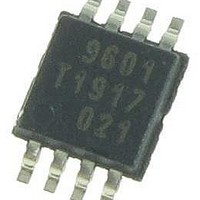
PCA9601DP,118 NXP Semiconductors, PCA9601DP,118 Datasheet - Page 16

PCA9601DP,118
Manufacturer Part Number
PCA9601DP,118
Description
IC DUAL BI-DIR BUS BUFFER 8-TSSO
Manufacturer
NXP Semiconductors
Datasheet
1.PCA9601D118.pdf
(31 pages)
Specifications of PCA9601DP,118
Number Of Channels Per Chip
2
Supply Voltage (max)
15 V
Supply Voltage (min)
2.5 V
Maximum Operating Temperature
+ 85 C
Mounting Style
SMD/SMT
Package / Case
TSSOP-8
Interface
I2C
Lead Free Status / RoHS Status
Lead free / RoHS Compliant
Other names
568-5302-2
Available stocks
Company
Part Number
Manufacturer
Quantity
Price
Company:
Part Number:
PCA9601DP,118
Manufacturer:
MAXIM
Quantity:
7 940
NXP Semiconductors
PCA9601_1
Product data sheet
Fig 18. Rising edge of SDA at slave is delayed by the buffers and bus rise times
V
CCM
MASTER
Effective delay of SDA at master: 115 + 0.2(Rs × Cs) + 0.7[(Rb × Cb) + (Rm × Cm)] (ns).
C = F; R = Ω.
I
2
C-BUS
local master bus
GND (0 V)
SDA
Figure
with relatively large capacitances linking two I
expressions for making the relevant timing calculations for 3.3 V or 5 V operation.
Because the buffers and the wiring introduce timing delays, it may be necessary to
decrease the nominal SCL frequency. In most cases the actual bus frequency will be
lower than the nominal Master timing due to bit-wise stretching of the clock periods.
The delay factors involved in calculation of the allowed bus speed are:
A — The propagation delay of the master signal through the buffers and wiring to the
slave. The important delay is that of the falling edge of SCL because this edge ‘requests’
the data or acknowledge from a slave. See
B — The effective stretching of the nominal LOW period of SCL at the master caused by
the buffer and bus rise times. See
C — The propagation delay of the slave's response signal through the buffers and wiring
back to the master. The important delay is that of a rising edge in the SDA signal. Rising
edges are always slower and are therefore delayed by a longer time than falling edges.
(The rising edges are limited by the passive pull-up while falling edges are actively
driven); see
The timing requirement in any I
provided in response to a falling edge of SCL) must be received at the master before the
end of the corresponding LOW period of SCL as appears on the bus wiring at the master.
Since all slaves will, as a minimum, satisfy the worst case timing requirements of their
speed class (Fast-mode, Fm+, etc.), they must provide their response, allowing for the
set-up time, within the minimum allowed clock LOW period, e.g., 450 ns (max.) for Fm+
parts. In systems that introduce additional delays it may be necessary to extend the
minimum clock LOW period to accommodate the ‘effective’ delay of the slave's response.
The effective delay of the slave’s response equals the total delays in SCL falling edge
16,
Rm
Cm
master bus
capacitance
Figure
V
Figure
SX
CCB
All information provided in this document is subject to legal disclaimers.
PCA9601
17, and
18.
Rev. 01 — 28 May 2010
Figure 18
TX/RX
buffered expansion bus
2
C-bus system is that a slave's data response (which is
Figure
Cb
buffered bus
wiring capacitance
Rb
show the PCA9601 used to drive extended bus wiring
TX/RX
17.
PCA9601
Figure
2
C-bus nodes. It includes simplified
16.
SX
Dual bidirectional bus buffer
Rs
Cs
slave bus
capacitance
remote slave bus
SDA
PCA9601
© NXP B.V. 2010. All rights reserved.
I
2
C-BUS
SLAVE
002aae882
V
CCS
16 of 31


