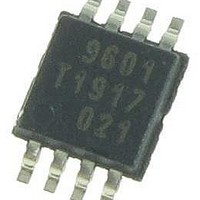
PCA9601DP,118 NXP Semiconductors, PCA9601DP,118 Datasheet - Page 5

PCA9601DP,118
Manufacturer Part Number
PCA9601DP,118
Description
IC DUAL BI-DIR BUS BUFFER 8-TSSO
Manufacturer
NXP Semiconductors
Datasheet
1.PCA9601D118.pdf
(31 pages)
Specifications of PCA9601DP,118
Number Of Channels Per Chip
2
Supply Voltage (max)
15 V
Supply Voltage (min)
2.5 V
Maximum Operating Temperature
+ 85 C
Mounting Style
SMD/SMT
Package / Case
TSSOP-8
Interface
I2C
Lead Free Status / RoHS Status
Lead free / RoHS Compliant
Other names
568-5302-2
Available stocks
Company
Part Number
Manufacturer
Quantity
Price
Company:
Part Number:
PCA9601DP,118
Manufacturer:
MAXIM
Quantity:
7 940
NXP Semiconductors
PCA9601_1
Product data sheet
7.2 High drive, long distance side
7.3 Connections to other bus buffers
The logic level on RX is determined from the power supply voltage V
LOW is below 40 % of V
threshold just slightly below half V
TX is an open-collector output without ESD protection diodes to V
via a pull-up resistor to a supply voltage in excess of V
exceeded. It has a larger current sinking capability than a normal I
able to sink a static current of greater than 30 mA, and typical 100 mA dynamic pull-down
capability as well.
A logic LOW is transmitted to TX when the voltage at I
logic LOW at RX will cause I
with I
looped back to the TX output and cause the buffer to latch LOW.
The LOW level this chip can achieve on the I
when sinking 1 mA.
If the supply voltage V
LOW. Their open-collector configuration allows them to be pulled up to the rated
maximum of 15 V even without V
presents no loading of external signals when V
The effective input capacitance of any signal pin, measured by its effect on bus rise times,
is less than 10 pF for all bus voltages and supply voltages including V
Two or more SX or SY I/Os must not be interconnected. The PCA9601 design does not
support this configuration. Bidirectional I
pin so, instead, slightly different logic LOW voltage levels are used at SX/SY to avoid
latching of this buffer. A ‘regular I
propagated to SX/SY as a ‘buffered LOW’ with a slightly higher voltage level. If this special
‘buffered LOW’ is applied to the SX/SY of another PCA9601, that second PCA9601 will
not recognize it as a ‘regular I
The SX/SY side of PCA9601 may not be connected to similar buffers that rely on special
logic thresholds for their operation, for example P82B96, PCA9511A, PCA9515A, ‘B’ side
of PCA9517, etc. The SX/SY side is only intended for, and compatible with, the normal
I
second PCA9601 or P82B96 if required. The TX/RX and TY/RY I/O pins use the standard
I
interconnection of the TX/RX and TY/RY I/O pins to other PCA9601s, for example in a
star or multipoint configuration with the TX/RX and TY/RY I/O pins on the common bus
and the SX/SY side connected to the line card slave devices. For more details see
Application Note AN10658, “Sending I
2
2
C-bus logic voltage levels of I
C-bus logic voltage levels of all I
2
C-bus requirements (maximum 1.5 V in 5 V applications) but not low enough to be
All information provided in this document is subject to legal disclaimers.
CC
Rev. 01 — 28 May 2010
CC
fails, then neither the I
, and logic HIGH is above 55 % of V
2
C-bus pin SX to be pulled to a logic LOW level in accordance
2
C-bus LOW’ and will not propagate it to its TX/TY output.
2
C-bus master and slave chips, or even TX/RX signals of a
2
CC
C-bus LOW’ applied at the RX/RY of a PCA9601 will be
2
CC
C-bus parts. There are no restrictions on the
present. The input configuration on SX and RX also
).
2
C-bus signals via long communication cables”.
2
C-bus signals do not allow any direction control
2
C-bus by a LOW at RX is typically 0.64 V
CC
2
C-bus nor the TX output will be held
is not present.
CC
2
C-bus pin SX is below 0.425 V. A
, as long as the 15 V rating is not
Dual bidirectional bus buffer
CC
CC
(with a typical switching
2
C-bus device, being
. It may be connected
CC
CC
PCA9601
© NXP B.V. 2010. All rights reserved.
of the chip. Logic
= 0 V.
5 of 31


