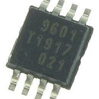
PCA9601DP,118 NXP Semiconductors, PCA9601DP,118 Datasheet - Page 17

PCA9601DP,118
Manufacturer Part Number
PCA9601DP,118
Description
IC DUAL BI-DIR BUS BUFFER 8-TSSO
Manufacturer
NXP Semiconductors
Datasheet
1.PCA9601D118.pdf
(31 pages)
Specifications of PCA9601DP,118
Number Of Channels Per Chip
2
Supply Voltage (max)
15 V
Supply Voltage (min)
2.5 V
Maximum Operating Temperature
+ 85 C
Mounting Style
SMD/SMT
Package / Case
TSSOP-8
Interface
I2C
Lead Free Status / RoHS Status
Lead free / RoHS Compliant
Other names
568-5302-2
Available stocks
Company
Part Number
Manufacturer
Quantity
Price
Company:
Part Number:
PCA9601DP,118
Manufacturer:
MAXIM
Quantity:
7 940
NXP Semiconductors
PCA9601_1
Product data sheet
from the master reaching the slave
SCL rising edge
SDA, reaching the master
The master microcontroller should be programmed to produce a nominal SCL LOW
period as follows:
The actual LOW period will become (the programmed value + the stretching time B).
When this actual LOW period is then less than the specified minimum, the specified
minimum should be used.
Example 1:
Example 2:
SCL LOW
It is required to connect an Fm+ slave, with Rs × Cs product of 100 ns, to a 5 V
Fast-mode system also having 100 ns Rm × Cm using two PCA9601’s to buffer a 5 V
bus with 4 nF loading and 160 Ω pull-up.
Calculate the allowed bus speed:
The maximum Fm+ slave response delay must be < 450 ns so the programmed LOW
period is calculated as:
The actual LOW period will be 887.5 + 285 = 1173 ns, which is below the Fast-mode
minimum, so the programmed LOW period must be increased to
(1300 − 285) = 1015 ns, so the actual LOW equals the 1300 ns requirement and this
shows that this Fast-mode system may be safely run to its limit of 400 kHz.
It is required to buffer a Master with Fm+ speed capability, but only 3 mA sink capability,
to an Fm+ bus. All the system operates at 3.3 V. The Master Rm × Cm product is 50 ns.
Only one PCA9601 is used. The Fm+ bus becomes the buffered bus. The Fm+ bus has
200 pF loading and 150 Ω pull-up, so its Rb × Cb product is 30 ns. The Fm+ slave has a
specified data valid time t
Calculate the allowed maximum system bus speed. (Note that the fixed values in the
delay equations represent the internal propagation delays of the PCA9601. Only one
PCA9601 is used here, so those fixed values used below are taken from the
characteristics.)
The delays are:
The programmed LOW period is calculated as:
Delay A = 120 + 85 + (2.5 + [4 × 4]) × 5 + 50 = 347.5 ns
Delay B = 115 + 100 + 70 = 285 ns
Delay C = 115 + 20 + 0.7(100 + 100) = 275 ns
LOW ≥ 450 + 347.5 − 285 + 275 + 100 = 887.5 ns
Delay A = 40 + 56 + (2.5 + [4 × 0.2]) × 3.3 = 107 ns
Delay B = 115 + 50 + 21 = 186 ns
Delay C = 70 + 0.7(50 + 30) = 126 ns
SCL LOW ≥ 300 + 117 − 186 + 126 + 50 = 407 ns
≥
(
slave response delay to valid data on its SDA
All information provided in this document is subject to legal disclaimers.
(Figure
Rev. 01 — 28 May 2010
17) plus total delays in the slave's response data, carried on
(Figure
VD;DAT
maximum of 300 ns.
18).
(Figure
16) minus the effective delay (stretch) of the
+
A B
–
Dual bidirectional bus buffer
+
C
+
data set-up time
PCA9601
© NXP B.V. 2010. All rights reserved.
)
17 of 31
ns
(1)


