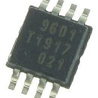
PCA9601DP,118 NXP Semiconductors, PCA9601DP,118 Datasheet - Page 19

PCA9601DP,118
Manufacturer Part Number
PCA9601DP,118
Description
IC DUAL BI-DIR BUS BUFFER 8-TSSO
Manufacturer
NXP Semiconductors
Datasheet
1.PCA9601D118.pdf
(31 pages)
Specifications of PCA9601DP,118
Number Of Channels Per Chip
2
Supply Voltage (max)
15 V
Supply Voltage (min)
2.5 V
Maximum Operating Temperature
+ 85 C
Mounting Style
SMD/SMT
Package / Case
TSSOP-8
Interface
I2C
Lead Free Status / RoHS Status
Lead free / RoHS Compliant
Other names
568-5302-2
Available stocks
Company
Part Number
Manufacturer
Quantity
Price
Company:
Part Number:
PCA9601DP,118
Manufacturer:
MAXIM
Quantity:
7 940
NXP Semiconductors
PCA9601_1
Product data sheet
Fig 20. Propagation SX to TX with V
Fig 22. Propagation RX to SX (SX pull-up to 3.3 V; V
V
(V)
CC
(1) TX output.
(2) SX input.
(1) RX input.
(2) SX output.
−1
7
6
5
4
3
2
1
0
0
(SX pull-up to 3.3 V; TX pull-up to 5.7 V)
100
10.2 Negative undershoot below absolute minimum value
200
300 400 500 600 700 800
(1)
(2)
The reason why the IC pin reverse voltage on pins TX and RX in
is specified at such a low value, −0.3 V, is not that applying larger voltages is likely to
cause damage but that it is expected that, in normal applications, there is no reason why
larger DC voltages will be applied. This ‘absolute maximum’ specification is intended to be
a DC or continuous ratings and the nominal DC I
even reach 0 V. Inside PCA9601 at every pin there is a large protective diode connected
to the GND pin and that diode will start to conduct when the pin voltage is more than about
−0.55 V with respect to GND at 25 °C ambient.
Figure 23
The plot was made using a curve tracer that applies 50 Hz mains voltage via a series
resistor, so the pulse durations are long duration (several milliseconds) and are reaching
peaks of over 2 A when more than −1.5 V is applied. The IC becomes very hot during this
V
(V)
CC
shows the measured characteristic for one of those diodes inside PCA9601.
−1
7
6
5
4
3
2
1
0
RX
0
All information provided in this document is subject to legal disclaimers.
002aac932
time (ns)
= V
100
CC
(1)
(2)
200
900
= 3.3 V
Rev. 01 — 28 May 2010
(1)
300 400 500 600 700 800
(2)
CC
= 3.3 V; RX pull-up to 4.6 V)
Fig 21. Propagation SX to TX with RX tied to TX;
V
(V)
CC
(1) TX/RX output.
(2) SX input.
−1
7
6
5
4
3
2
1
0
0
V
5.7 V)
CC
(1)
002aac934
time (ns)
100
= 3.3 V (SX pull-up to 3.3 V; TX pull-up to
(2)
2
(2)
C-bus voltage LOW usually does not
200
900
(1)
300 400 500 600 700 800
(2)
Dual bidirectional bus buffer
Table 5 “Limiting values”
PCA9601
© NXP B.V. 2010. All rights reserved.
002aac933
time (ns)
(1)
(2)
900
19 of 31


