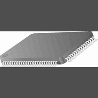
CR16MCS9VJE8 National Semiconductor, CR16MCS9VJE8 Datasheet - Page 54

CR16MCS9VJE8
Manufacturer Part Number
CR16MCS9VJE8
Description
16-Bit Microcontroller IC
Manufacturer
National Semiconductor
Datasheet
1.CR16MCS9VJE8.pdf
(156 pages)
Specifications of CR16MCS9VJE8
Controller Family/series
CR16X
Core Size
16 Bit
Program Memory Size
64K X 8 Flash
Digital Ic Case Style
PQFP
No. Of Pins
80
Mounting Type
Surface Mount
Clock Frequency
25MHz
Lead Free Status / RoHS Status
Contains lead / RoHS non-compliant
Available stocks
Company
Part Number
Manufacturer
Quantity
Price
Company:
Part Number:
CR16MCS9VJE8
Manufacturer:
ON
Quantity:
8 917
Company:
Part Number:
CR16MCS9VJE8-CBB
Manufacturer:
ON
Quantity:
846
Company:
Part Number:
CR16MCS9VJE8-CBC
Manufacturer:
ON
Quantity:
109
Company:
Part Number:
CR16MCS9VJE8-CBD
Manufacturer:
ON
Quantity:
17
Company:
Part Number:
CR16MCS9VJE8-CBE
Manufacturer:
ON
Quantity:
1 950
www.national.com
counter or to operate in the pulse accumulate mode because
the TnB input is used as a capture input. Attempting to select
one of these configurations will cause one or both counters
to stop. In this mode, Timer/Counter II must be enabled at all
times.
15.3
Each Multi-Function Timer unit has four interrupt sources,
designated A, B, C, and D. Interrupt sources A, B, and C are
mapped into a single system interrupt called Timer Interrupt
I, while interrupt source D is mapped into a system interrupt
called Timer Interrupt II. Each of the four interrupt sources
has its own enable bit and pending flag. The enable flags are
named TnAIEN, TnBIEN, TnCIEN, and TnDIEN. The pend-
ing flags are named TnAPND, TnBPND, TnCPND, and TnD-
PND.
For Multi-Function Timer unit MFT1, Timer Interrupts I and II
are system interrupts T1A and T1B (IRQ13 and IRQ12), re-
spectively. For Multi-Function Timer unit MFT2, Timer Inter-
rupts I and II are system interrupts T2A and T2B (IRQ11 and
IRQ10), respectively.
Table15 shows the events that trigger interrupts A, B, C, and
D in each of the four operating modes. Note that some inter-
rupt sources are not used in some operating modes, as indi-
cated by the notation “N/A” (Not Applicable) in the table.
15.4
Each Multi-Function Timer unit uses two I/O pins, called T1A
and T1B (for Timer MFT1) or T2A and T2B (for Timer MFT2).
The function of each pin depends on the timer operating
mode and the TnAEN and TnBEN enable bits. Table16
Timer I
Clock
Timer II
Clock
TIMER INTERRUPTS
TIMER I/O FUNCTIONS
Figure 17. Mode 4: Input Capture Plus Timer Block Diagram
Timer/Counter I
Timer/Counter II
TnCNT1
Capture B
Reload A
TnCRA
TnCRB
TnCNT2
Underflow
Preset
54
shows the functions of the pins in each operating mode, and
for each combination of enable bit settings.
When pin TnA is configured to operate as a PWM output
(TnAEN = 1), the state of the pin is toggled on each underflow
of the TnCNT1 counter. In this case, the initial value on the
pin is determined by the TnAOUT bit. For example, to start
with TnA high, the software should set the TnAOUT bit to 1
prior to enabling the timer clock. This option is available only
when the timer is configured to operate in Mode 1, 3, or 4 (in
other words, when TnCRA is not used in Capture mode).
TnBEN
TnAPND
TnBPND
TnDPND
TnBIEN
TnAIEN
TnDIEN
TnATEN
Interrupt I
Interrupt I
Interrupt II
Timer
Timer
Timer
TnA
TnB


