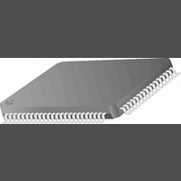
CR16MCS9VJE8 National Semiconductor, CR16MCS9VJE8 Datasheet - Page 56

CR16MCS9VJE8
Manufacturer Part Number
CR16MCS9VJE8
Description
16-Bit Microcontroller IC
Manufacturer
National Semiconductor
Datasheet
1.CR16MCS9VJE8.pdf
(156 pages)
Specifications of CR16MCS9VJE8
Controller Family/series
CR16X
Core Size
16 Bit
Program Memory Size
64K X 8 Flash
Digital Ic Case Style
PQFP
No. Of Pins
80
Mounting Type
Surface Mount
Clock Frequency
25MHz
Lead Free Status / RoHS Status
Contains lead / RoHS non-compliant
Available stocks
Company
Part Number
Manufacturer
Quantity
Price
Company:
Part Number:
CR16MCS9VJE8
Manufacturer:
ON
Quantity:
8 917
Company:
Part Number:
CR16MCS9VJE8-CBB
Manufacturer:
ON
Quantity:
846
Company:
Part Number:
CR16MCS9VJE8-CBC
Manufacturer:
ON
Quantity:
109
Company:
Part Number:
CR16MCS9VJE8-CBD
Manufacturer:
ON
Quantity:
17
Company:
Part Number:
CR16MCS9VJE8-CBE
Manufacturer:
ON
Quantity:
1 950
15.5
The following CPU-accessible registers are used to control
the Multi-Function Timers:
15.5.1
The Clock Prescaler (TnPRSC) register is a byte-wide, read/
write register that holds the current value of the 5-bit clock
prescaler (CLKPS). This register is cleared upon reset. The
register format is shown below.
15.5.2
The Clock Unit Control (TnCKC) register is a byte-wide, read/
write register that selects the clock source for each timer/
counter. Selecting the clock source also starts the counter.
This register is cleared upon reset, which disables the timer/
counters. The register format is shown below.
C1CSEL
C2CSEL
CLKPS
Reserved
— Clock Prescaler Register (TnPRSC)
— Clock Unit Control Register (TnCKC)
— Timer/Counter I Register (TnCNT1)
— Timer/Counter II Register (TnCNT2)
— Reload/Capture A Register (TnCRA)
— Reload/Capture B Register (TnCRB)
— Timer Mode Control Register (TnCTRL)
— Timer Interrupt Control Register (TnICTL)
— Timer Interrupt Clear Register (TnICLR)
7
7
Reserved
Clock Prescaler Register (TnPRSC)
Clock Unit Control Register (TnCKC)
TIMER REGISTERS
6
6
Clock Prescaler. When the timer is configured
to use the prescaled clock, the system clock is
divided by CLKPS+1 to produce the timer
clock. Thus, the system clock divide-by factor
can range from 1 to 32.
Counter I Clock Select. This 3-bit field defines
the clock mode for Timer/Counter I as follows:
000 = no clock (timer/counter I stopped)
001 = prescaled system clock
010 = external event on TnB (modes 1 and 3
only)
011 = pulse accumulate mode based on TnB
(modes 1 and 3 only)
100 = slow clock *
other values = undefined
Counter II Clock Select. This 3-bit field defines
the clock mode for Timer/Counter II as follows:
000 = no clock (Timer/Counter II stopped
modes 1, 2, and 3 only)
001 = prescaled system clock
010 = external event on TnB (modes 1 and 3
only)
011 = pulse accumulate mode based on TnB
(modes 1 and 3 only)
100 = slow clock *
other values = undefined
5
5
C2CSEL
4
4
3
3
CLKPS
2
2
C1CSEL
1
1
0
0
56
* Operation of the slow clock is determined by the CRC-
TRL.SCLK control bit, as described in Section12.6.1.
15.5.3
The Timer/Counter I (TnCNT1) register is a word-wide, read/
write register that holds the current count value for Timer/
Counter I. The register contents are not affected by a reset
and are unknown upon power-up.
15.5.4
The Timer/Counter II (TnCNT2) register is a word-wide, read/
write register that holds the current count value for Timer/
Counter II. The register contents are not affected by a reset
and are unknown upon power-up.
15.5.5
The Reload/Capture A (TnCRA) register is a word-wide,
read/write register that holds the reload or capture value for
Timer/Counter I. The register contents are not affected by a
reset and are unknown upon power-up.
15.5.6
The Reload/Capture B (TnCRB) register is a word-wide,
read/write register that holds the reload or capture value for
Timer/Counter II. The register contents are not affected by a
reset and are unknown upon power-up.
15.5.7
The Timer Mode Control (TnCTRL) register is a byte-wide,
read/write register that sets the operating mode of the timer/
counter and the TnA and TnB pins. This register is cleared
upon reset. The register format is shown below.
MDSEL
TnAEDG
TnBEDG
TnAEN
Reserved TnAOUT
7
Timer/Counter I Register (TnCNT1)
Timer/Counter II Register (TnCNT2)
Reload/Capture A Register (TnCRA)
Reload/Capture B Register (TnCRB)
Timer Mode Control Register (TnCTRL)
6
Mode Select. This 2-bit field sets the operating
mode of the timer/counter as follows:
00 = Mode 1: PWM plus system timer
01 = Mode 2: Dual Input Capture plus system
timer
10 = Mode 3: Dual Timer/Counter
11 = Mode 4: Single Input Capture and Single
Timer
TnA Edge Polarity. When cleared (0), input pin
TnA is sensitive to falling edges (high to low
transitions). When set (1), input pin TnA is sen-
sitive to rising edges (low to high transitions).
TnB Edge Polarity. When cleared (0), input pin
TnB is sensitive to falling edges (high to low
transitions). When set (1), input pin TnB is sen-
sitive to rising edges (low to high transitions). In
pulse accumulate mode, when this bit is set (1),
the counter is enabled only when TnB is high;
when this bit is cleared (0), the counter is en-
abled only when TnB is low.
TnA Enable. When set (1), the TnA pin is en-
abled to operate as a preset input or as a PWM
output, depending on the timer operating
mode. In Mode 2 (Dual Input Capture), a tran-
sition on the TnA pin presets the TnCNT1
counter to FFFF hex. In the other modes, TnA
functions as a PWM output. When this bit is
TnBEN
5
TnAEN
4
TnBEDG TnAEDG
3
2
www.national.com
1
MDSEL
0


