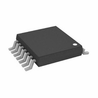
AD5280BRUZ200 Analog Devices Inc, AD5280BRUZ200 Datasheet - Page 14

AD5280BRUZ200
Manufacturer Part Number
AD5280BRUZ200
Description
IC,Digital Potentiometer,TSSOP,14PIN,PLASTIC
Manufacturer
Analog Devices Inc
Datasheet
1.AD5280BRUZ50.pdf
(28 pages)
Specifications of AD5280BRUZ200
Taps
256
Resistance (ohms)
200K
Number Of Circuits
1
Temperature Coefficient
30 ppm/°C Typical
Memory Type
Volatile
Interface
I²C, 2-Wire Serial
Voltage - Supply
4.5 V ~ 16.5 V, ±4.5 V ~ 5.5 V
Operating Temperature
-40°C ~ 85°C
Mounting Type
Surface Mount
Package / Case
14-TSSOP
Resistance In Ohms
200K
Lead Free Status / RoHS Status
Lead free / RoHS Compliant
AD5280/AD5282
THEORY OF OPERATION
The AD5280/AD5282 are single-channel and dual-channel,
256-position, digitally controlled variable resistors (VRs). To
program the VR settings, see the Digital Interface section. Both
parts have an internal power-on preset that places the wiper at
midscale during power-on, which simplifies the fault condition
recovery at power-up. Operation of the power-on preset function
also depends on the state of the V
RHEOSTAT OPERATION
The nominal resistance of the RDAC between Terminal A and
Terminal B is available in 20 kΩ, 50 kΩ, and 200 kΩ. The final
two or three digits of the part number determine the nominal
resistance value, for example, 20 kΩ = 20, 50 kΩ = 50, and
200 kΩ = 200. The nominal resistance (R
256 contact points accessed by the wiper terminal, plus the B
terminal contact. The eight-bit data in the RDAC latch is
decoded to select one of the 256 possible settings. Assuming
that a 20 kΩ part is used, the wiper’s first connection starts at
the B terminal for data 0x00. Because there is a 60 Ω wiper
contact resistance, such a connection yields a minimum of 60 Ω
resistance between Terminal W and Terminal B.
The second connection is the first tap point that corresponds to
138 Ω (R
third connection is the next tap point representing 216 Ω (78 ×
2 + 60) for data 0x02, and so on. Each LSB data value increase
moves the wiper up the resistor ladder until the last tap point is
reached at 19,982 Ω (R
simplified diagram of the equivalent RDAC circuit where the
last resistor string is not accessed; therefore, there is 1 LSB less
of the nominal resistance at full scale in addition to the wiper
resistance.
WB
Figure 44. AD5280/AD5282 Equivalent RDAC Circuit
= R
SHDN
AB
DECODER
D7
D6
D5
D4
D3
D2
D1
D0
LATCH
/256 + R
RDAC
AND
AB
– 1 LSB + R
W
R
R
R
R
S
S
S
S
= 78 Ω + 60 Ω) for data 0x01. The
0xFF
0x01
0x00
L
pin.
SW
A
W
SW
). Figure 46 shows a
B
AB
) of the VR has
A
W
B
X
X
X
Rev. C | Page 14 of 28
The general equation determining the digitally programmed
output resistance between W and B is
where:
D is the decimal equivalent of the binary code loaded in the 8-
bit RDAC register.
R
R
the internal switch.
Note that in the zero-scale condition, a finite wiper resistance
of 60 Ω is present. Care should be taken to limit the current
flow between W and B in this state to a maximum pulse current
of no more than 20 mA. Otherwise, degradation or possible
destruction of the internal switch contact can occur.
As in the mechanical potentiometer, the resistance of the RDAC
between Wiper W and Terminal A also produces a digitally
controlled complementary resistance, R
are used, the B terminal can be opened. Setting the resistance
value for R
decreases as the data loaded in the latch increases in value. The
general equation for this operation is
The typical distribution of the nominal resistance, R
channel to channel matches within ±1%. Device-to-device
matching is process lot dependent, and it is possible to have a
±30% variation. Because the resistance element is processed in
thin film technology, the change in R
small (30 ppm/°C).
POTENTIOMETER OPERATION
The digital potentiometer easily generates a voltage divider at
wiper to B and wiper to A to be proportional to the input voltage
at A to B. Unlike the polarity of V
positive, voltage across A to B, W to A, and W to B can be at
either polarity, provided that V
If the effect of the wiper resistance for approximation is ignored,
connecting the A terminal to 5 V and the B terminal to ground
produces an output voltage at the wiper to B starting at 0 V up
to 1 LSB less than 5 V. Each LSB of voltage is equal to the
voltage applied across A to B divided by the 256 positions of the
potentiometer divider. Because the AD5280/AD5282 can be
supplied by dual supplies, the general equation defining the
output voltage at V
AB
W
is the wiper resistance contributed by the on resistance of
is the nominal end-to-end resistance.
R
R
WB
WA
( )
( )
D
D
WA
starts at a maximum value of resistance and
=
=
256
256
D
256
W
×
−
with respect to ground for any valid
R
D
AB
×
+
R
AB
R
W
+
SS
R
is powered by a negative supply.
W
DD
– V
AB
WA
with temperature is very
SS
. When these terminals
, which must be
AB
, from
(1)
(2)


