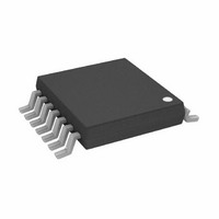
AD5280BRUZ200 Analog Devices Inc, AD5280BRUZ200 Datasheet - Page 20

AD5280BRUZ200
Manufacturer Part Number
AD5280BRUZ200
Description
IC,Digital Potentiometer,TSSOP,14PIN,PLASTIC
Manufacturer
Analog Devices Inc
Datasheet
1.AD5280BRUZ50.pdf
(28 pages)
Specifications of AD5280BRUZ200
Taps
256
Resistance (ohms)
200K
Number Of Circuits
1
Temperature Coefficient
30 ppm/°C Typical
Memory Type
Volatile
Interface
I²C, 2-Wire Serial
Voltage - Supply
4.5 V ~ 16.5 V, ±4.5 V ~ 5.5 V
Operating Temperature
-40°C ~ 85°C
Mounting Type
Surface Mount
Package / Case
14-TSSOP
Resistance In Ohms
200K
Lead Free Status / RoHS Status
Lead free / RoHS Compliant
AD5280/AD5282
APPLICATIONS INFORMATION
BIPOLAR DC OR AC OPERATION FROM DUAL
SUPPLIES
The AD5280/AD5282 can be operated from dual supplies
enabling control of ground-referenced ac signals or bipolar
operation. The ac signal, as high as V
directly across Terminal A to Terminal B with the output taken
from Terminal W. See Figure 55 for a typical circuit connection.
GAIN CONTROL COMPENSATION
The digital potentiometer is commonly used in gain control
applications such as the noninverting gain amplifier shown in
Figure 56.
Notice that the RDAC B terminal parasitic capacitance is
connected to the op amp noninverting node. It introduces a 0
for the 1/β
amp GBP has −20 dB/dec characteristics. A large R2 and finite
C1 can cause the 0 frequency to fall well below the crossover
frequency. Thus the rate of closure becomes 40 dB/dec, and the
system has a 0° phase margin at the crossover frequency. The
output may ring or oscillate if the input is a rectangular pulse or
step function. Similarly, it is also likely to ring when switching
between two gain values because this is equivalent to a step
change at the input.
MICROCONTROLLER
GND
V
DD
O
SCLK
MOSI
Figure 55. Bipolar Operation from Dual Supplies
term with 20 dB/decade (dec), whereas a typical op
Figure 56. Typical Noninverting Gain Amplifier
47kΩ
R
1
C
1
25pF
V
SCL
SDA
GND
B
I
AD5282
U1
V
200kΩ
4.7pF
SS
C2
W
DD
/V
A
SS
, can be applied
A
W
B
A
W
B
V
1
1
2
2
O
1
2
±2.5V p-p
D–80
H
–5.0V
+5.0V
±5V p-p
Rev. C | Page 20 of 28
Depending on the op amp GBP, reducing the feedback resistor
may extend the zero’s frequency far enough to overcome the
problem. A better approach is to include a compensation
capacitor C2 to cancel the effect caused by C1. Optimum
compensation occurs when R1 × C1 = R2 × C2. This is not
an option unless C2 is scaled as if R2 were at its maximum
value. Doing so may overcompensate and compromise the
performance slightly when R2 is set at low values. However, it
avoids the gain peaking, ringing, or oscillation at the worst case.
For critical applications, C2 should be found empirically to suit
the need. In general, C2 in the range of a few picofarads (pF) to
no more than a few tenths of a picofarad is usually adequate for
the compensation.
Similarly, there are W and A terminal capacitances connected to
the output (not shown); fortunately, their effect at this node is less
significant and the compensation can be avoided in most cases.
15 V, 8-BIT I
ADR512
AD5280/AD5282 can be configured as a high voltage DAC, as
high as 15 V. The output is
R
BIAS
V
O
V
(
DD
D
D1
)
=
R1
256
2
D
C DAC
AD8512
1 [
V–
V+
2 .
V
R2
DD
Figure 57. 8-Bit I
V
U1A
×
1 (
+
R
R
2
1
U2
AD5280
)]
B
2
C DAC
200kΩ
U1B
AD8512
V
(5)
O


