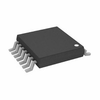
AD5280BRUZ200 Analog Devices Inc, AD5280BRUZ200 Datasheet - Page 21

AD5280BRUZ200
Manufacturer Part Number
AD5280BRUZ200
Description
IC,Digital Potentiometer,TSSOP,14PIN,PLASTIC
Manufacturer
Analog Devices Inc
Datasheet
1.AD5280BRUZ50.pdf
(28 pages)
Specifications of AD5280BRUZ200
Taps
256
Resistance (ohms)
200K
Number Of Circuits
1
Temperature Coefficient
30 ppm/°C Typical
Memory Type
Volatile
Interface
I²C, 2-Wire Serial
Voltage - Supply
4.5 V ~ 16.5 V, ±4.5 V ~ 5.5 V
Operating Temperature
-40°C ~ 85°C
Mounting Type
Surface Mount
Package / Case
14-TSSOP
Resistance In Ohms
200K
Lead Free Status / RoHS Status
Lead free / RoHS Compliant
8-BIT BIPOLAR DAC
Figure 58 shows a low cost, 8-bit, bipolar DAC. It offers the same
number of adjustable steps but not the precision of conventional
DACs. The linearity and temperature coefficients, especially at
low value codes, are skewed by the effects of the digital potenti-
ometer wiper resistance. The output of this circuit is
BIPOLAR PROGRAMMABLE GAIN AMPLIFIER
For applications that require bipolar gain, Figure 59 shows one
implementation similar to the previous circuit. The digital
potentiometer, U
at W
given U
linear gain and attenuation. The transfer function is
where K is the ratio of R
2
V
V
V
GND
V
V
V
can therefore be programmed between V
IN
1
O
O
i
1
2
AD5282
=
V
TRIM
=
setting. Configuring A
U
OUT
ADR425
⎛ 2
⎜
⎝
U
1
⎛
⎜
⎝
AD5282
2
Figure 59. Bipolar Programmable Gain Amplifier
1
256
D
+
U
1
+5V
R2
R1
−
A
A
1
2
1
, sets the adjustment range. The wiper voltage
1
REF
⎞
⎟
⎠
⎞
⎟
⎠
W
B
W
A
×
Figure 58. 8-Bit Bipolar DAC
×
B
2
1
2
1
V
1
+
OP2177
–
⎛
⎜
⎝
R
REF
256
D2
WB1
B
U
V+
V–
V
2
V
DD
S8
/R
×
W
WA1
(
A
1
OP2177
A
–
+
R
+15V
1
2
–15V
+
in noninverting mode allows
set by U
K
–kVI
)
−
A
K
U
+
OP2177
–
2
2
–5V
1
⎞
⎟
⎠
–
.
V+
V–
AD5280
V
V
OP2177
+
–
REF
DD
S8
+15V
–15V
A
C1
i
2
A
and –KV
2
R2
R1
V
i
V
O
at a
O
Rev. C | Page 21 of 28
(6)
(7)
As in the previous example, in the simpler and more common
case where K = 1, a single digital AD5280 potentiometer is
used. U
V
relationship becomes
If R2 is large, a compensation capacitor having a few pF may be
needed to avoid any gain peaking.
Table 7 shows the result of adjusting D, with A2 configured as a
unity gain, a gain of 2, and a gain of 10. The result is a bipolar
amplifier with linearly programmable gain and a 256-step
resolution.
Table 7. Result of Bipolar Gain Amplifier
D
0
64
128
192
255
PROGRAMMABLE VOLTAGE SOURCE WITH
BOOSTED OUTPUT
For applications that require high current adjustments, such as a
laser diode driver or tunable laser, a boosted voltage source can
be considered (see Figure 60).
In this circuit, the inverting input of the op amp forces the
V
ometer. The load current is then delivered by the supply via the
N-channel FET N1. The N1 power handling must be adequate
to dissipate (V
maximum of 100 mA with a 5 V supply. A1 needs to be a rail-
to-rail input type. For precision applications, a voltage reference
such as ADR423, ADR292, or
input of the digital potentiometer.
i
BIAS
V
5V
and −V
I
U
V
1
to be equal to the wiper voltage set by the digital potenti-
O
1
A
B
=
is replaced by a matched pair of resistors to apply
R1 = ∞, R2 = 0
−1
−0.5
0
0.5
0.968
i
W
⎛
⎜
⎝
at the ends of the digital potentiometer. The
Figure 60. Programmable Booster Voltage Source
1
+
+
–
i
R2
– V
R1
A1
⎞
⎟
⎠
O
⎛
⎜
⎝
) × I
V+
V–
2
256
D2
L
power. This circuit can source a
−
1
⎞
⎟
⎠
AD1584
×
V
i
R1 = R2
−2
−1
0
1
1.937
SIGNAL
U
A
N
1
1
1
AD5280/AD5282
= AD5280
= FDV301N, 2N7002
= AD8501, AD8605, AD8541
can be applied at the
C
C
R
BIAS
R2 = 9R1
−10
−5
0
5
9.680
V
O
I
L
(7)


